Santa Clara, Calif. — Feb. 18, 2026 — As AI models scale toward trillion-parameter regimes and agentic AI workloads proliferate, the semiconductor industry is entering a phase where traditional design methodologies can no longer keep pace. Speaking at today’s Chiplet Summit 2026, Synopsys Fellow Abhijeet Chakraborty argued that AI must now be applied not just on silicon, but to silicon engineering itself—an approach he described as “AI for AI.”
The explosive growth of AI is driving a rapid shift toward large, heterogeneous, multi-die systems. While advanced packaging has enabled this transition, Chakraborty noted that the resulting design complexity—spanning system partitioning, power delivery, die-to-die interconnects, software co-design, reliability, and security—is increasing faster than human-driven engineering workflows can absorb. Late-stage design changes are especially costly, both in time-to-results and in silicon re-spins, making early, predictive decision-making critical.
Advanced Packaging Enters a “Golden Era”
Chakraborty described the current period as a “golden era” for advanced packaging innovation, driven by the goal of making die-to-die connectivity approach the bandwidth, latency, and energy efficiency of on-die interconnects. Achieving monolithic-like behavior across chiplets remains the industry’s “holy grail,” but rapid progress is being made across multiple packaging approaches.
Today’s landscape includes embedded silicon bridges, ultra-high-density fanout technologies, 2.5D silicon interposers, 3D stacked memory, and logic-on-logic stacking. Looking ahead, panel-level packaging is emerging as a major inflection point, with square and rectangular panels potentially reaching 310 × 310 mm—and eventually 620 × 620 mm—enabling far larger systems while lowering cost per die by improving utilization compared to round wafers.
These advances are reflected in market growth. The global semiconductor packaging market reached roughly $47 billion in 2025 and is projected to exceed $155 billion within the next eight years, representing a CAGR of approximately 16.5%, fueled largely by AI accelerators and chiplet-based architectures.
Multi-Die Systems Multiply Design Challenges
As AI systems scale, so does design complexity. Chakraborty highlighted the growing number of architectural decision points—from node selection and bump density to UCIe-based die-to-die connectivity, streaming protocol choices, substrate selection, and packaging trade-offs. Power delivery has become one of the most critical constraints, where both over-design and under-design can introduce cascading costs and performance penalties.
Beyond hardware, software-hardware co-design is now mandatory. Software bring-up and debug increasingly drive hardware changes, reinforcing the need to surface these interactions early in the design cycle. At the system level, AI data centers demand extreme reliability, predictive thermal management, and lifecycle analytics across thousands of GPUs, CPUs, sensors, and interconnects. Security further complicates matters, as multi-vendor chiplet supply chains require authentication, secure key exchange, and protection in multi-tenant environments.
How Synopsys Applies AI to Engineering Itself
To address these challenges, Chakraborty outlined how Synopsys has progressively embedded AI across EDA workflows. Early use of reinforcement learning improved performance, power, and area optimization in physical design and analog circuits, while also reducing test counts and accelerating verification. Data analytics layers were added to enhance silicon lifecycle management, fab efficiency, and yield learning.
More recently, large and small language models have enabled assistive and generative capabilities—from knowledge assistants that elevate junior engineers to automated assertion generation, testbench creation, and RTL mutation. According to Chakraborty, these tools already deliver measurable gains in productivity and quality of results.
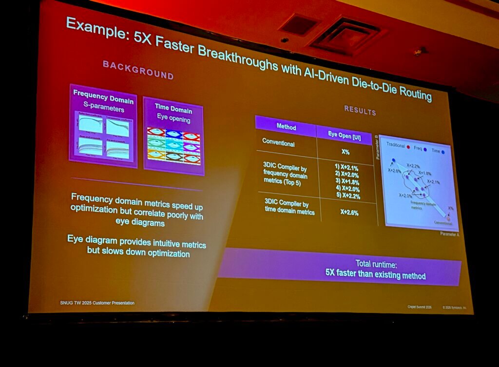
Looking forward, the next phase is agentic AI—coordinated teams of AI “engineers” capable of planning, executing, and iterating across complex, multi-step design problems. In examples cited, physics-informed AI dramatically reduced search space for die-to-die channel routing, achieving superior signal-integrity results in weeks rather than months. In verification, AI enabled higher coverage with roughly three times fewer test cases than traditional constrained-random methods.
AI-Driven Autonomy Levels for Multi-Die Design (Synopsys)
AI-Driven Autonomy Levels for Multi-Die Design
| Autonomy Level | Capability Description |
|---|---|
| L1 – Assistive | Human engineers define objectives and make key decisions, with AI providing guidance, optimization suggestions, and workflow assistance. |
| L2 – Partial Autonomy | AI agents autonomously execute well-scoped tasks, such as fixing a specific class of DRC violations or performing localized optimizations. |
| L3 – Coordinated Autonomy | Multiple AI agents collaborate to resolve complex issues requiring changes across layout, routing, TSVs, and related design elements. |
| L4 – Planned Autonomy | AI systems plan and orchestrate fixes across hundreds or thousands of interdependent issues, optimizing solutions holistically while managing trade-offs. |
| L5 – Full Autonomy | AI engineers independently solve complex, multi-step design problems end-to-end with minimal human intervention. |
Autonomous Engineering as an Industry Imperative
Chakraborty concluded that autonomous, AI-driven engineering is no longer optional for chiplet-based AI systems—it is essential. As designs grow larger, more heterogeneous, and more tightly constrained by cost, power, reliability, and security, only AI-assisted and AI-autonomous workflows can meet aggressive time-to-results targets.
He called on designers, architects, business leaders, and ecosystem partners to work together on standards, interoperability, and shared best practices—arguing that the industry now has a rare opportunity to shape the future of multi-die engineering and agentic AI innovation.