Toshiba Begins Construction of 3D Flash Memory Fab
Toshiba started construction of a new state-of-the-art semiconductor fabrication and a new Memory R&D center at Yokkaichi Operations in Mie prefecture, Japan, the company’s main memory production base.
Fab 6 will be dedicated to production of Toshiba’s 3D BiCS FLASH, which promises significant density improvements over planar NAND Flash memory.
http://www.toshiba.com
Share this article
Help others discover this reporting.
Editorial responsibility
Staff
Editor & Publisher
Every article published by Converge Digest is researched, curated, fact-checked and editorially reviewed by Jim Carroll, Editor & Publisher. AI-assisted drafting may be used to accelerate production, but all content is reviewed, refined and approved prior to publication.
You just read about Flash. Here is what it replaced:
EPROM (UV-erasable) served 1971–2000. What ultimately replaced it?
EPROM (UV-erasable) floating-gate ROM erased by shining ultraviolet light through a quartz window, then reprogrammed on a special programmer. Its job passed to Flash — but the problem it solved, and the ideas it proved, live on in what replaced it. The standard rests here in the archive. One of 198 technologies here that opened a door and then held it for the next.

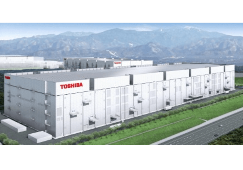
 Toshiba started construction of a new state-of-the-art semiconductor fabrication and a new Memory R&D center at Yokkaichi Operations in Mie prefecture, Japan, the company’s main memory production base.