• Home
  • About
  • Events Calendar
  • Blueprint Guidelines
  • Privacy Policy
  • Manage Email Delivery
  • NextGenInfra.io
No Result
View All Result
Converge Digest
Saturday, June 6, 2026
  • Home
  • About
  • Events Calendar
  • Blueprint Guidelines
  • Privacy Policy
  • Manage Email Delivery
  • NextGenInfra.io
No Result
View All Result
Converge Digest
No Result
View All Result

Home » SCALE Photonics Spins Out of Sony with Ultra-Compact High-Peak Laser 

SCALE Photonics Spins Out of Sony with Ultra-Compact High-Peak Laser 

April 20, 2026
in Optical, Start-ups
A A

Silicon Catalyst Japan K.K. has selected SCALE photonics Inc., a spin-off from Sony Semiconductor Solutions, as the first project for both its incubation program and affiliated investment fund. The Tokyo-based accelerator will back the newly formed startup as it moves to commercialize a chip-scale “ultra-compact high-peak laser,” marking a milestone for Japan’s efforts to bring advanced semiconductor innovations out of large corporate R&D environments and into standalone ventures.

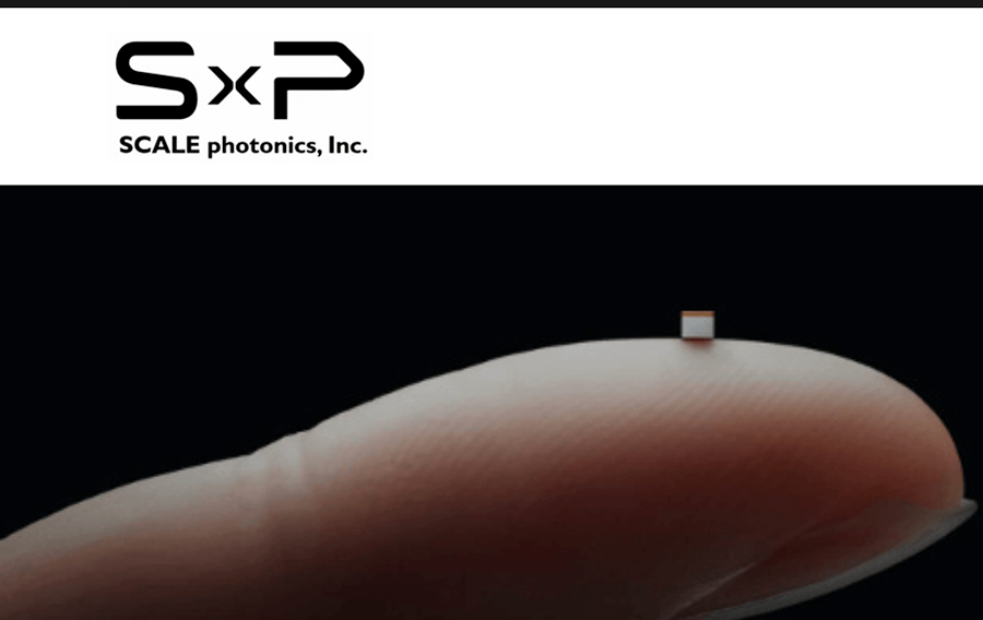
SCALE photonics’ core technology integrates light-emitting semiconductor materials with solid-state laser gain media on a single chip. The device measures approximately 1 mm³ (0.04 in³) and delivers peak output of 57 kW, addressing a long-standing tradeoff between compact semiconductor lasers and high-power solid-state systems. Traditional high-power lasers require large assemblies of precision optical components, while the new approach aims to enable wafer-level manufacturing of high-output lasers in a compact, low-cost form factor.

The company targets applications including high-precision sensing and emerging “Physical AI” systems, where compact, high-power optical sources could enable new classes of machine perception. Silicon Catalyst Japan said the investment reflects its strategy to unlock dormant intellectual property within Japanese corporations and accelerate commercialization through global partnerships and venture funding.

  • SCALE photonics spun out of Sony Semiconductor Solutions in January 2026
  • First incubation and investment project for Silicon Catalyst Japan
  • Chip-scale laser integrates semiconductor and solid-state materials on one die
  • Device size: ~1 mm³ (0.04 in³) with peak output of 57 kW
  • Enables wafer-level manufacturing vs. traditional assembled laser systems
  • Targets sensing, industrial, and Physical AI applications
  • SCJ aims to replicate model for additional deep-tech spin-offs in Japan

“With our unique ‘ultra-compact high-peak laser’ technology that defies conventional tradeoffs, we will contribute to applications such as high-precision sensing for Physical AI,” said Masanao Kamata, CEO of SCALE photonics.

🌐 Analysis: The SCALE photonics spin-off reflects a broader push in Japan to translate long-developed corporate R&D into venture-backed startups, similar to spin-out trends seen in the U.S. and Europe. Silicon Catalyst Japan’s involvement mirrors global accelerator models that pair capital with ecosystem access to accelerate semiconductor commercialization.

🌐 Analysis: On the technology side, chip-scale integration of high-peak laser sources could have implications for sensing, LiDAR, and advanced optical systems, particularly as AI-driven physical environments demand more compact and power-efficient photonic components. The approach aligns with industry trends toward photonic integration and wafer-scale manufacturing, which are also shaping silicon photonics and optical interconnect markets.

🌐 We’re tracking the latest developments in semiconductors and photonics. Follow our ongoing coverage at: https://convergedigest.com/category/semiconductors/

Tags: Japan
ShareTweetShareSummarizeSummarize
Previous Post

Ericsson Q1 2026: Networks Growth Offsets Enterprise Losses Amid FX Headwinds

Next Post

Accelsius Debuts 150kW Rack-Scale Two-Phase Cooling 

Jim Carroll

Jim Carroll

Editor and Publisher, Converge! Network Digest, Optical Networks Daily - Covering the full stack of network convergence from Silicon Valley

Related Posts

Signature: whKF177fklf7qGBqH5MkMhmEGtoOHPAyfLDZ958fBhmoxzvbFRg39DGBUMJ80VskXDUDkXVEfcQuQuLRYQUiFZrX93f4JaNMU2JplhlgcvVpUSG47flbf3uXz63tWRUyLGcOOQvVzoZqwNRLlra8DNHlAHj7U3YYyloW7LJTX0yGiFrJKdNvwPU6XcD7XCgkLmh1i9TP1ifo34IbJ9JdrzXBcgSZ4ZYfu0QfJS0TO8rKiu+QHIZM2u1ZIRRgMLJIIWz6YBqhfsZudTNR3pm2GXqvnCAb9xjLNLj944z05xc=
5G / 6G / Wi-Fi

Ericsson and KDDI Complete AI-Driven Uplink Optimization Trial

May 11, 2026
Enterprise

NEC Taps Anthropic Claude to Build Large-Scale AI Engineering 

April 25, 2026
AI Infrastructure

NTT DATA Opens 30MW Keihanna Data Center

April 9, 2026
Data Centers

Digital Realty Expands Tokyo AI Footprint with 100 MW NRT Campus

April 8, 2026
5G / 6G / Wi-Fi

SoftBank Taps Ericsson Cloud-Native Core to Drive 5G SA 

March 26, 2026
Space

NTT Unveils 192-Core Multicore Subsea Cable System 

March 25, 2026
Next Post

Accelsius Debuts 150kW Rack-Scale Two-Phase Cooling 

Categories

  • 5G / 6G / Wi-Fi
  • AI Infrastructure
  • All
  • Automotive Networking
  • Blueprints
  • Clouds and Carriers
  • Data Centers
  • Enterprise
  • Explainer
  • Feature
  • Financials
  • Last Mile / Middle Mile
  • Legal / Regulatory
  • Optical
  • Quantum
  • Research
  • Security
  • Semiconductors
  • Space
  • Start-ups
  • Subsea
  • Sustainability
  • Video
  • Webinars

Archives

Tags

5G All AT&T Australia AWS Blueprint columns BroadbandWireless Broadcom China Ciena Cisco Data Centers Dell'Oro Ericsson FCC Financial Financials Huawei Infinera Intel Japan Juniper Last Mile Last Mille LTE Mergers and Acquisitions Mobile NFV Nokia Optical Packet Systems PacketVoice People Regulatory Satellite SDN Service Providers Silicon Silicon Valley StandardsWatch Storage TTP UK Verizon Wi-Fi
Converge Digest

A private dossier for networking and telecoms

Follow Us

  • Home
  • About
  • Events Calendar
  • Blueprint Guidelines
  • Privacy Policy
  • Manage Email Delivery
  • NextGenInfra.io

© 2026 Converge Digest - A private dossier for networking and telecoms.

No Result
View All Result
  • Home
  • About
  • Events Calendar
  • Blueprint Guidelines
  • Privacy Policy
  • Manage Email Delivery
  • NextGenInfra.io

© 2026 Converge Digest - A private dossier for networking and telecoms.

This website uses cookies. By continuing to use this website you are giving consent to cookies being used. Visit our Privacy and Cookie Policy.
Go to mobile version