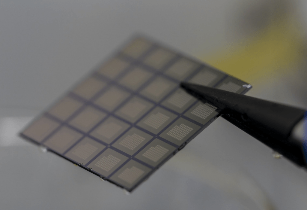
Syenta, an Australia-founded semiconductor startup focused on advanced packaging, raised $26 million in Series A funding to commercialize its chip-to-chip interconnect technology for AI systems. The round was led by Playground Global and Australia’s National Reconstruction Fund, with participation from existing investors Investible, Salus Ventures, Jelix Ventures, and Wollemi Capital. The company said the financing will support commercialization, U.S. expansion, and preparation for high-volume production.
The company positions its technology at one of AI infrastructure’s growing pain points: the limits of advanced packaging. As AI systems scale toward larger multi-die and chiplet-based designs, performance increasingly depends on how efficiently chips exchange data. Syenta says its proprietary Localized Electrochemical Manufacturing, or LEM, process enables high-density chip-to-chip connections while avoiding a redesign of existing manufacturing infrastructure, a claim that directly targets concerns around packaging complexity, cost, and capacity concentration.
Syenta said its early results show micron-scale interconnects, 40% fewer process steps, and improved manufacturing efficiency. The company, which emerged from research at the Australian National University, is also establishing a presence in Arizona as it moves closer to U.S. semiconductor customers and packaging initiatives. Pat Gelsinger, general partner at Playground Global and former Intel CEO, will join Syenta’s board as part of the investment.
- Series A funding: $26 million
- Total funding to date: more than $36 million
- Lead investors: Playground Global and Australia’s National Reconstruction Fund
- Other participants: Investible, Salus Ventures, Jelix Ventures, Wollemi Capital
- Focus: advanced packaging and chip-to-chip connectivity for AI systems
- Core technology: Localized Electrochemical Manufacturing (LEM)
- Claimed benefits: micron-scale interconnects, 40% fewer process steps, no redesign of existing manufacturing infrastructure required
- Origin: founded from research at the Australian National University
- U.S. expansion: building a presence in Arizona
- Board update: Pat Gelsinger joins Syenta’s board of directors
“Today’s advanced packaging approaches have real limits on interconnect density, which constrain the bandwidth between chips,” said Dr. Jekaterina Viktorova, CEO and founder of Syenta. “We’re enabling finer-pitch connections within existing manufacturing infrastructure, allowing systems to move more data more efficiently and at a lower cost without requiring entirely new fabrication approaches.”
🌐 Analysis: Syenta is entering a strategic part of the AI hardware stack where advanced packaging, substrate capacity, and interconnect density now shape system-level performance as much as the logic die itself. Its pitch stands out because it focuses on “standardizing” high-density interconnects inside existing packaging flows. By providing a “stamp-like” electrochemical process that avoids the bottlenecks of traditional photolithography, Syenta offers a path to scale chiplet architectures without the extreme capital expenditure typically required for new advanced packaging lines.
| Profile: Syenta | |
|---|---|
| Company | Syenta |
| Founded | 2020 (originated as Spark3D spin-out from Australian National University) |
| Headquarters | Sydney, Australia (expanding presence in Arizona, USA) |
| Website | www.syenta.com |
| Business Model | Fabless advanced packaging and chip-to-chip interconnect technology provider |
| Core Technology | Localized Electrochemical Manufacturing (LEM), an additive electrochemical process for high-density interconnect fabrication |
| Technical Approach | Electrochemical additive manufacturing using proprietary functional inks to deposit multi-material structures (metals, polymers, semiconductors) layer-by-layer |
| Key Advantages | Micron-scale interconnects; ~40% fewer process steps; reduced need for etching and masking; compatible with existing manufacturing infrastructure |
| AI Infrastructure Role | Enables higher bandwidth, lower-latency chip-to-chip communication for GPU, XPU, and HBM integration in large-scale AI systems |
| Funding | $26 million Series A (April 2026); total funding exceeds $36 million |
| Key Investors | Playground Global; Australia’s National Reconstruction Fund (NRF); Investible; Salus Ventures; Jelix Ventures; Wollemi Capital |
| Board | Pat Gelsinger (Board Member, joined 2026) |
| Ecosystem Engagement | Validated through industry programs; working with semiconductor equipment providers; supported by Semiconductor Service Bureau (S3B) |
| Value Proposition | Improves interconnect density and manufacturability while reducing cost, process complexity, and dependence on specialized packaging fabs |
| Applications | Advanced semiconductor packaging, chiplets, heterogeneous integration, AI accelerators, potential expansion into printed sensors and electronic components |
| Strategic Focus (2026) | Commercialization, scaling production equipment, and integration into OSAT manufacturing environments globally |
🌐 We’re tracking the latest developments in networking silicon. Follow our ongoing coverage at: https://convergedigest.com/category/semiconductors/