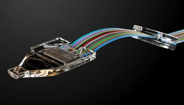
Lam Research and CEA–Leti signed a new multi-year research agreement aimed at accelerating the development of next-generation specialty semiconductor devices with improved energy efficiency. The collaboration targets emerging applications spanning MEMS, 3D imaging and sensing, power management, RF, photonics—including MicroLED displays—and optical interconnect technologies.
The partners will focus on pathfinding new multi-element materials and fabrication processes for compound semiconductors, with an emphasis on reducing power consumption while improving performance for AI and high-performance computing workloads. Lam will apply its etch and deposition platforms, including pulsed laser deposition, alongside CEA-Leti’s materials analysis and device characterization capabilities to shorten the cycle from process innovation to functional validation.
Building on prior co-development work, including pulsed plasma technologies, the joint program will explore novel films and integration schemes for specialty devices such as RF filters, electro-optic modulators, and quantum-optics components. The companies say the effort is designed to surface integration challenges earlier and deliver fabrication solutions that are closer to industrial readiness.
- Multi-year R&D agreement focused on specialty semiconductor technologies
- Target domains include MEMS, RF, photonics, optical interconnects, and quantum optics
- Emphasis on new materials and lower-power compound semiconductor processes
- Combines Lam’s etch/deposition platforms with CEA-Leti’s characterization and pre-industrialization facilities
“As we enter the AI era, the opportunities for Specialty Technology are immense,” said Vahid Vahedi, chief technology and sustainability officer at Lam Research, adding that the collaboration aims to “fast-track the development of new, ground-breaking advancements and future generations of more energy-efficient and higher-performance Specialty Technology devices.”
🌐 Analysis
The agreement extends Lam’s long-running strategy of pairing process-tool development with advanced research institutes to de-risk new materials before they reach high-volume manufacturing. It also aligns with broader industry efforts to improve energy efficiency in specialty and heterogeneous devices as RF, photonics, and optical interconnects become more tightly coupled to AI and data-center architectures.