At the PIC Summit, Nick Harris, founder and CEO of Lightmatter, delivered a keynote built around a clear conclusion: the next major order-of-magnitude gains in AI system performance will come not from GPUs alone, but from re-architecting the network using photonics.
Harris opened by observing that the last roughly thousand-fold improvement in AI performance has been driven primarily by advances in compute. While foundry process scaling has played a role, he argued that the dominant factor has been reduced numerical precision—moving from FP32 to FP16, FP8, and now FP4. That trajectory, he said, is nearing its practical limits. Modern AI systems increasingly function as distributed supercomputers, where overall performance is governed by how efficiently data moves between compute elements. From a physics standpoint, Harris argued, the next thousand-fold improvement must come from communication rather than arithmetic, and specifically from photonic interconnects.

A central theme of the talk was the widening imbalance between compute density and I/O capability. Harris traced how chip sizes have expanded over time, from roughly centimeter-scale dies two decades ago to today’s multi-thousand-square-millimeter devices. Compute scales with die area, but I/O scales with die perimeter. Because high-speed SerDes must sit at the edge of a chip for signal-integrity reasons, the ability to move data off-chip has not kept pace with the growth of on-chip compute. Harris presented this mismatch as a fundamental motivation for photonics: while compute capability has increased by orders of magnitude over the past 30 years, interconnect bandwidth has advanced far more slowly.
He connected these physical constraints to contemporary AI cluster design. In today’s architectures, fast communication occurs within scale-up domains, while scale-out networks between pods are significantly slower. According to Harris, AI architects work hard to keep workloads within the fast scale-up region, because crossing into scale-out paths introduces sharp performance penalties. Copper interconnects, he said, can realistically support on the order of hundreds of GPUs before running into distance and shoreline limits, while customer roadmaps toward the end of the decade point to per-GPU I/O requirements approaching 100 Tb/s.
Harris then outlined how Lightmatter views the photonics roadmap. The industry began with pluggable optical modules operating at 800G and 1.6T, but those devices are constrained by power density and form factor. Near-packaged optics (NPO) reduce energy per bit by shortening electrical paths and simplifying SerDes. Beyond that lies co-packaged optics (CPO) on advanced packaging platforms, followed by photonic interposers that allow communication across the full surface of a chip rather than only around its edges. Harris said Lightmatter is actively developing products across NPO, CPO, and interposer-based architectures, all implemented in silicon today.
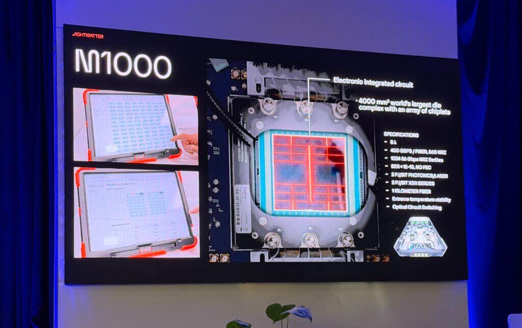
As a concrete example, Harris highlighted Lightmatter’s Passage platform. Passage M1000 delivers approximately 114 Tb/s on a single chip and supports up to 2.5 kW of power delivery per package, corresponding to power densities around 1.4 W/mm². Built using advanced 3D integration, Passage places compute stacks directly on top of a dense photonic I/O layer. Harris emphasized that optical circuit switching is integrated into Passage, enabling lane remapping, redundancy, and isolation of failed nodes—capabilities he described as important for reliability in co-packaged optical systems at scale.
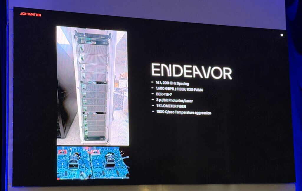
He also detailed Lightmatter’s Bobcat and Endeavor platforms, which focus on bidirectional optical links. By combining transmit and receive paths onto a single fiber, bidirectional optics reduce fiber count and lower total cost of ownership. Bobcat delivers 800 Gb/s per fiber using NRZ signaling, with raw bit-error rates on the order of 10⁻¹⁰ without forward error correction. Endeavor doubles that bandwidth to 1.6 Tb/s per fiber using PAM4 signaling. Across these platforms, Harris cited measured energy efficiencies of roughly 2.6 to 3 picojoules per bit for the photonics and laser components, operation over fiber lengths up to one kilometer, and tolerance to rapid temperature excursions.
Harris presented system-level results from a Lightmatter paper that received a Best Industry Paper award at Hot Interconnects. Using a modeled 576-GPU cluster with 32 Tb/s of I/O per GPU, the analysis showed that photonic scale-up networks significantly reduced training time for mixture-of-experts workloads. As the number of experts increased from 32 to 256, the Passage-enabled architecture achieved training-time improvements ranging from about 1.5× to 2.7× compared with a conventional multi-pod alternative. Harris framed these gains as the result of alleviating communication bottlenecks rather than changes to model architecture.
Throughout the keynote, Harris avoided prescribing a single “correct” link format. He noted that Lightmatter supports multiple generations—56G, 112G, 224G, and 448G—and both standards-compliant links, such as DR4, and custom DWDM designs. He identified 224G as a likely crossover point for many deployments, while noting that some customers are evaluating 448G and others are prioritizing lower-latency DWDM links at lower per-lane rates. All Lightmatter links, he said, are compatible with bidirectional operation.
Harris closed by reflecting on Lightmatter’s trajectory since its founding at MIT in 2017. He described the company’s early years as focused on articulating the vision for photonic computing and interconnect, and the current phase as one of execution—delivering manufacturable, reliable silicon rather than “PowerPoint photonics.” The emphasis, he said, has shifted to engineering rigor and deployment at scale, as photonics moves from promise to production in AI infrastructure.