At PIC Summit USA in Sunnyvale, Andy Bechtelsheim, co-founder and chief architect of Arista Networks, argued that the rapid scaling of AI models is pushing data center networks into what he described as an “AI networking moment,” where existing interconnect approaches are no longer sufficient.
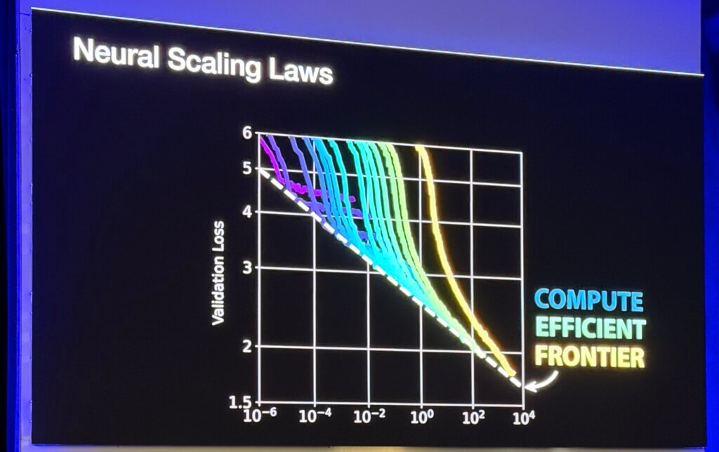
Bechtelsheim grounded his argument in neural scaling behavior: as model accuracy improves, the incremental gains require orders of magnitude more compute and, critically, more communication bandwidth. This dynamic, combined with growing model sizes, mixtures of experts, and ever-larger datasets, is driving demand for dramatically higher scale-up bandwidth inside tightly coupled GPU clusters. He noted that today’s systems deliver on the order of ~12.8 Tb/s of scale-up bandwidth per GPU, with near-term roadmaps doubling that figure and longer-term requirements reaching toward ~100 Tb/s per device. At data center scale, he said, this implies aggregate bandwidth measured not in petabits, but ultimately exabits—levels that cannot be supported economically with conventional optical architectures.
A central point in Bechtelsheim’s talk was that copper remains the dominant solution for scale-up networks today, largely because of cost, availability, and power efficiency. Hyperscalers, he noted, are extending copper as far as physics allows by building larger, higher-power racks—sometimes in the megawatt class—rather than prematurely transitioning to optics that would cost more than the compute they interconnect. As a result, optics must improve by roughly an order of magnitude in cost, density, and power efficiency to displace copper in scale-up environments.
He outlined two broad architectural paths: “slow and wide” approaches that trade speed for power efficiency, and the mainstream “fast and narrow” path that continues to push higher per-lane data rates. Bechtelsheim characterized the industry’s move toward 400G-class lanes as likely one of the final steps for traditional electrical scaling, with further gains becoming increasingly difficult.
Turning to optics, Bechtelsheim emphasized that while silicon photonics has made significant progress, it does not scale geometrically in the way CMOS does. He briefly referenced graphene-based technology as a post-silicon approach layered on standard silicon that could enable much higher optical density via tightly spaced DWDM, describing it as a potential long-term path rather than a production solution.
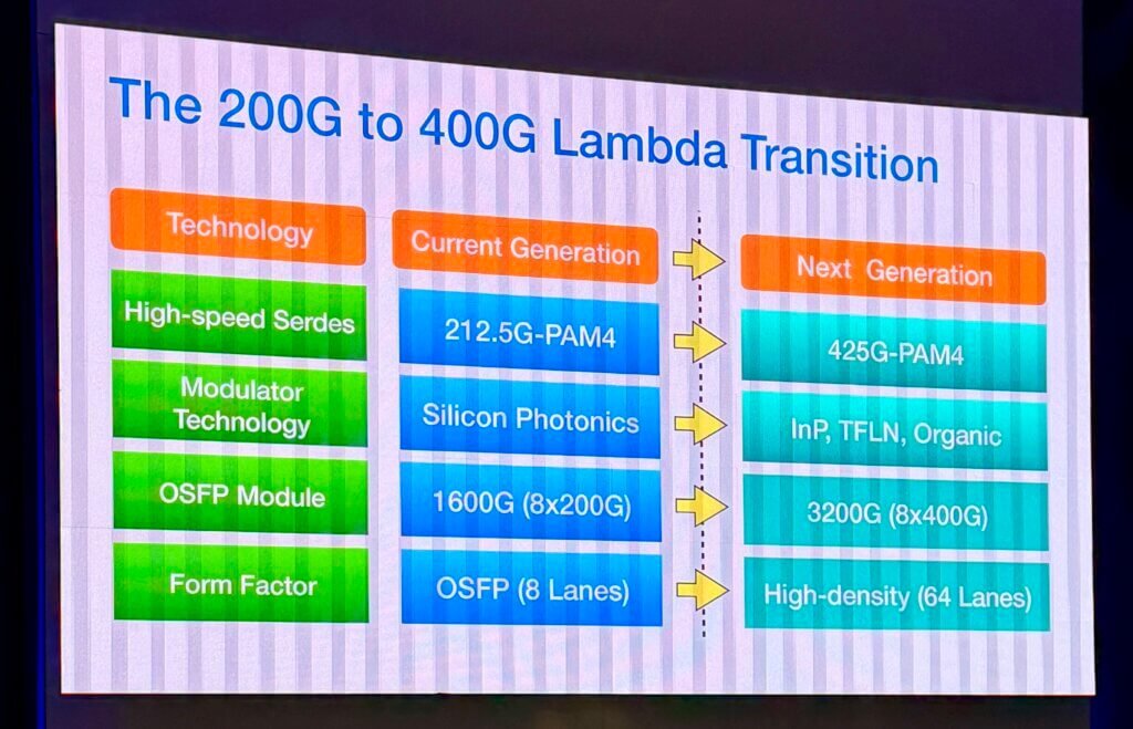
Much of his discussion focused on practical, near-term evolution. He highlighted the transition from 200G-PAM4 to 400G-PAM4 per lane, noting that PAM6 may benefit copper channels due to lower Nyquist bandwidth, but is less attractive for optics because of OSNR penalties and the high power cost of PAM6-to-PAM4 gearbox DSPs. As a result, he stressed the importance of native PAM4 SerDes at 400G-class speeds for optical systems.
Bechtelsheim reviewed Arista’s view of emerging optical modules, including 1.6T and 3.2T designs based on 400G-PAM4 lambdas, with production timelines extending toward the 2028 timeframe. He underscored that higher per-lane speeds can reduce overall system power by cutting the number of optical engines, fibers, and interfaces required, even as absolute bandwidth increases.
Power efficiency was a recurring theme. Bechtelsheim pointed to reductions in SerDes power enabled by advanced process nodes, as well as lower optical power consumption from newer modulator technologies. He noted that VCSEL and RF/microwave approaches can achieve very low power but are typically limited in reach, making them more suitable for short-reach scale-up links. For now, he said, co-packaged optics remains closely tied to silicon photonics, while pluggable optics offer flexibility to adopt multiple emerging low-power technologies as they mature.
Finally, Bechtelsheim addressed manufacturability, emphasizing that scaling to tens or hundreds of millions of optical modules per year requires highly automated production lines with minimal manual intervention. In his view, the economics of AI infrastructure depend as much on manufacturing scale and yield as on raw performance.
Throughout the keynote, Bechtelsheim framed the challenge facing the industry in pragmatic terms: moving bits is inherently expensive in power and cost, and every watt spent on interconnect is a watt not available for computation. The task ahead, he suggested, is not to abandon copper prematurely, but to make optics dense, efficient, and manufacturable enough that it becomes the obvious next step for AI-scale networks.