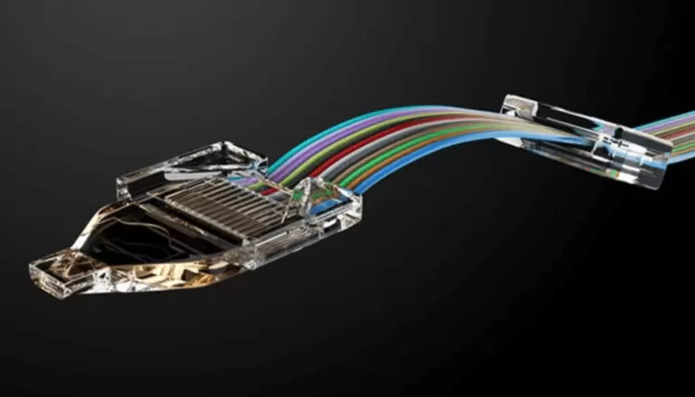
Peter Smyth, CEO of X-Celeprint, discusses how microtransfer printing technology addresses critical challenges in heterogeneous integration for silicon photonics and other advanced applications. Smyth explains the importance of precision placement at the nanometer scale and reveals how his company’s approach impacts device performance, power consumption, and manufacturing economics.
He shares insights into X-Celeprint’s customer engagement model, production achievements, and the expanding ecosystem of partners enabling volume manufacturing. The discussion covers real-world adoption metrics and the strategic advantages driving early market adoption by vertically integrated players.

- How microtransfer printing achieves 100-nanometer alignment precision for delicate component placement
- The relationship between placement accuracy and device performance, power consumption, and reliability
- Why vertically integrated companies are leading adoption of this technology
- Current production scale capabilities and yield achievements in silicon photonics manufacturing
- X-Celeprint’s equipment platform and customer engagement approach
- The growing partner ecosystem spanning foundries, device manufacturers, and OSAT providers • Real-world applications across silicon photonics, laser production, and data storage
Have a tech update that you want to brief us on? Contact [email protected]!
Check out other Tech Updates on our YouTube Channel (subscribe today): https://www.youtube.com/@NextGenInfra and check out our latest reports at: https://nextgeninfra.io/