Camtek Ltd. secured a $31 million multi-system order from a leading OSAT, with systems targeted primarily at CoWoS-like advanced packaging flows supporting AI processors. The company reported that total orders from leading OSAT customers in Q1 2026 have already surpassed $90 million, with the majority tied to similar high-performance packaging applications.
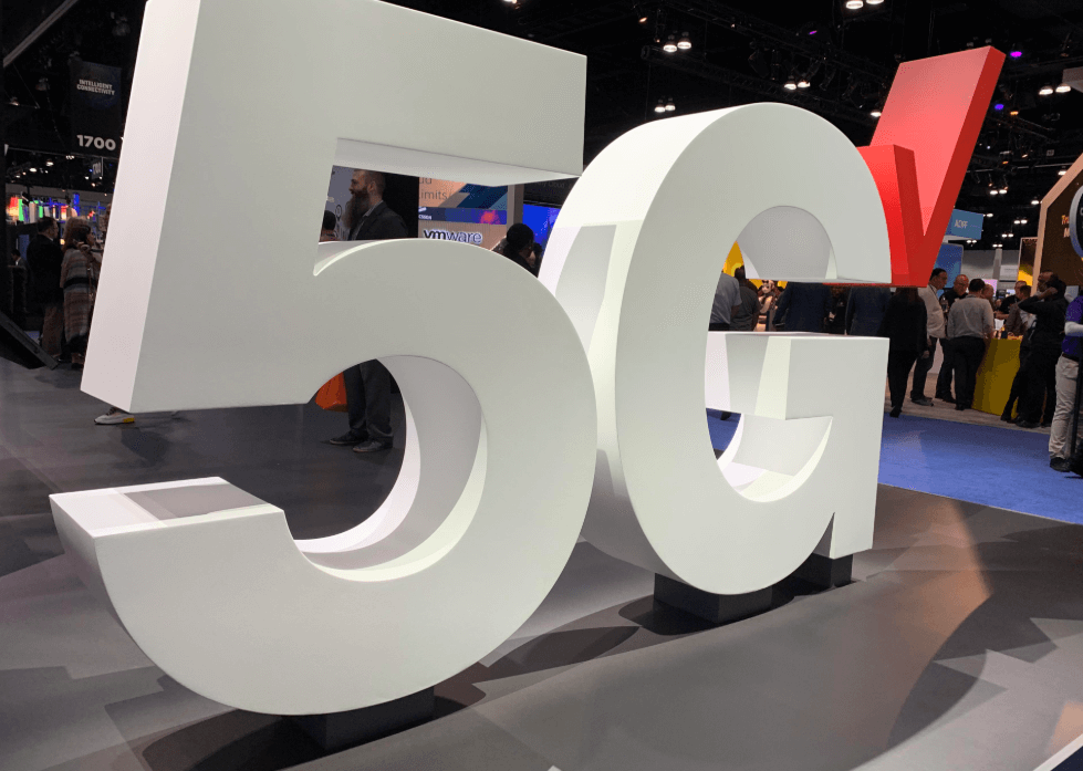
The order highlights accelerating demand for inspection and metrology tools in heterogeneous integration environments, particularly those resembling CoWoS architectures. These packaging schemes, widely associated with AI accelerators and HBM integration, require high-precision optical inspection across multiple process steps, including wafer-level redistribution layers (RDL), hybrid bonding interfaces, and post-dicing stages. Camtek’s systems address defect detection and critical dimension measurement challenges across these increasingly complex packaging stacks.
The growing role of OSATs (Outsourced Semiconductor Assembly and Test providers) reflects a structural shift in the AI semiconductor supply chain, where advanced packaging capacity has become a gating factor for deployment of next-generation GPUs and AI ASICs. Camtek indicated that the ordered systems are scheduled for delivery within 2026, supporting continued capacity expansion among OSAT customers focused on AI-driven workloads.
- $31 million multi-system order from a leading OSAT focused on AI packaging
- Q1 2026 cumulative orders from OSATs exceed $90 million
- Majority of demand tied to CoWoS-like advanced packaging architectures
- Systems support inspection and metrology across wafer-level and post-dicing processes
- Deliveries expected throughout 2026 to support capacity ramp
Rafi Amit, CEO of Camtek, said the surge in orders “underscores our observation that OSATs are playing an increasingly central role in the advanced packaging market for AI applications… Camtek is uniquely positioned to support this growing demand with our advanced inspection and metrology capabilities.”
🌐 Analysis: The order momentum aligns with broader industry expansion around advanced packaging, where players such as Taiwan Semiconductor Manufacturing Company have scaled CoWoS capacity to meet AI accelerator demand from companies like NVIDIA. Inspection and metrology vendors are becoming critical enablers as defect sensitivity increases with multi-die integration and HBM stacking.
Camtek Ltd. is an Israel-based provider of inspection and metrology equipment for advanced semiconductor manufacturing, with headquarters in Migdal HaEmek, Israel. The company’s mission centers on enabling yield optimization and process control for increasingly complex semiconductor devices, particularly in advanced packaging and heterogeneous integration. Camtek’s core technology portfolio includes high-resolution optical inspection systems and AI-driven defect detection platforms tailored for front-end wafer fabrication and back-end advanced packaging, including fan-out wafer-level packaging (FOWLP) and CoWoS-like architectures used in AI accelerators.
Founded in 1987 and publicly traded on NASDAQ (CAMT) and the Tel Aviv Stock Exchange, Camtek is led by CEO Rafi Amit, who has emphasized expansion into high-growth segments such as high-bandwidth memory (HBM) and advanced packaging for AI workloads. The company’s product lines—such as the Eagle and Hawk inspection platforms—are widely deployed by leading OSATs (outsourced semiconductor assembly and test providers) and IDMs.
🌐 Analysis: The concentration of orders among OSATs also signals continued outsourcing of advanced packaging beyond traditional foundries, with OSATs investing heavily to capture AI-related growth—creating sustained demand for process control equipment across the packaging ecosystem.
| CoWoS (Chip-on-Wafer-on-Substrate): Technical Overview and Industry Status (2026) | ||
|---|---|---|
| Category | Technical Details | Current Status (2026) |
| Definition | Chip-on-Wafer-on-Substrate (CoWoS) is a 2.5D advanced packaging architecture that integrates multiple dies (logic + HBM) on a silicon interposer with high-density interconnects. | Widely adopted for AI accelerators and high-performance computing (HPC) devices. |
| Interconnect Technology | Uses silicon interposers with fine-pitch TSVs (Through-Silicon Vias) and micro-bumps (~40–55µm pitch) to enable high bandwidth (>Tbps class die-to-die links). | Scaling toward hybrid bonding and finer pitches (<10µm roadmap) to support next-gen AI workloads. |
| Memory Integration | Enables tight integration of HBM stacks (HBM3/3E/4) adjacent to compute die, delivering extremely high memory bandwidth (>3–5 Tbps per package). | Critical enabler for AI GPUs (e.g., large language model training and inference). |
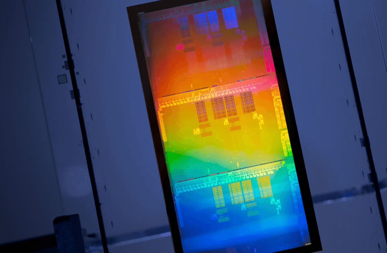
| Process Complexity | Multi-step flow including wafer thinning, TSV formation, RDL layers, die placement, and high-precision bonding; requires advanced inspection and metrology at each step. | Yield management is a major challenge; inspection intensity increasing significantly. |
| Thermal & Power | High power density due to stacked memory and large compute die; requires advanced cooling (liquid cooling, cold plates). | Thermal constraints are now a key limiter in AI system scaling. |
| Manufacturing Ecosystem | Historically dominated by foundries; now expanding to OSATs with capabilities in interposers, advanced substrates, and heterogeneous integration. | Rapid OSAT investment; supply chain diversification underway. |
| Capacity Constraints | Limited interposer fabrication, advanced substrate supply, and packaging throughput. | Major bottleneck for AI chip shipments; capacity expansions ongoing through 2026–2027. |
| Alternatives / Evolution | Competing approaches include chiplets with organic substrates, fan-out packaging, and 3D stacking (hybrid bonding, direct die stacking). | Transition toward CoWoS-L, CoWoS-R, and full 3D integration architectures underway. |
| Inspection & Metrology | Requires sub-micron defect detection across RDL layers, TSVs, bonding interfaces, and post-dicing stages. | Fast-growing segment; critical to yield improvement and cost control in AI packaging. |
🌐 We’re tracking the latest developments in networking silicon. Follow our ongoing coverage at: https://convergedigest.com/category/semiconductors/