Etched raised $300 million in new funding at a $10.3 billion valuation to accelerate production of its custom AI inference systems, expand manufacturing, and build infrastructure designed for gigawatt-scale AI deployments. The financing was led by Sequoia Capital with participation from Andreessen Horowitz, Jane Street, Diffusion, Argo, and SK hynix.
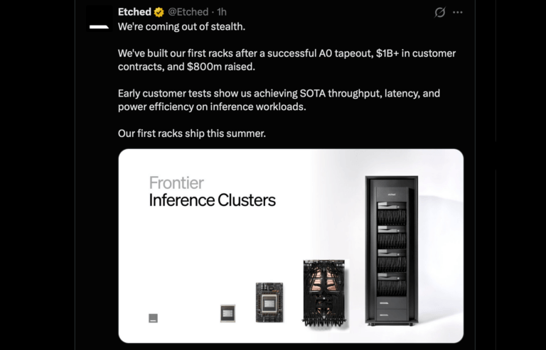
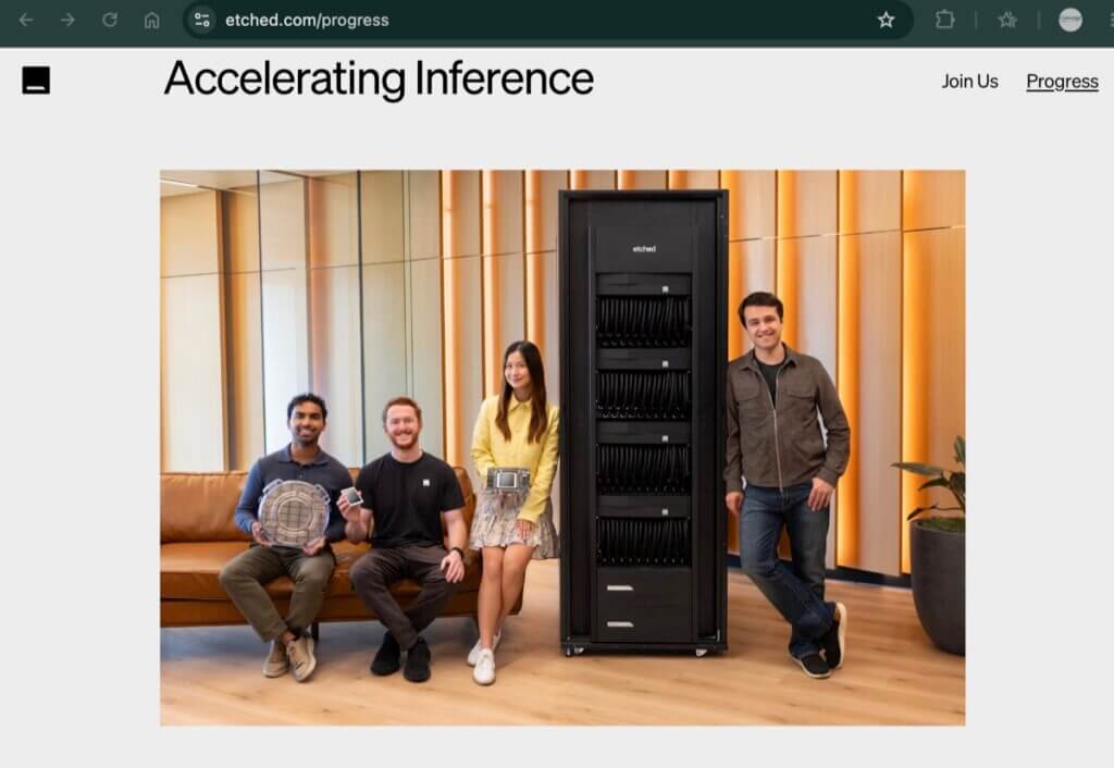
The San Jose-based company said it has begun fabrication of “hundreds of millions of dollars” worth of inference clusters and recently completed a new 10-megawatt hardware validation laboratory located near its headquarters. The facility supports continuous deployment of first-generation systems while accelerating development of future hardware generations. Etched said it is vertically integrating much of its engineering effort, spanning custom silicon, advanced packaging, printed circuit boards, cold plates, interconnects, software, and manufacturing. The company expects its first production racks to ship this summer as it works to satisfy more than $1 billion in customer demand.
Etched positions its systems specifically for frontier AI inference rather than AI training. Earlier this year the company received first silicon fabricated on TSMC’s N4P process and announced two key architectural technologies: Low Voltage Inference (LVI), which operates compute blocks at significantly lower voltage to improve sustained throughput while reducing thermal throttling, and Cluster Scale Memory (CSM), a shared HBM/SRAM memory architecture connected through a proprietary ultra-low-latency interconnect. According to Etched, the architecture targets large mixture-of-experts (MoE), long-context, and agentic AI workloads while improving throughput, latency, and power efficiency.
| Etched: Key Technical & Business Metrics | |
| New Funding | $300 million |
| Valuation | $10.3 billion |
| Lead Investor | Sequoia Capital |
| Additional Investors | Andreessen Horowitz, Jane Street, Diffusion, Argo, SK hynix |
| Customer Commitments | More than $1 billion |
| Engineering Team | 400+ engineers |
| Silicon | First-generation A0 chip fabricated on TSMC N4P |
| Validation Lab | 10 MW hardware development facility |
| Target Market | Frontier AI inference clusters |
| Key Technologies | Low Voltage Inference (LVI), Cluster Scale Memory (CSM) |
| Production Status | First production racks scheduled to ship summer 2026 |
“Our mission is to run the world’s inference,” the company said. “Frontier models deserve frontier inference clusters: co-designed chips, packages, PCBs, cold plates, interconnects, and more that push the entire Pareto curve on the most demanding workloads.”
🌐 Analysis
Etched continues to differentiate itself from GPU vendors by focusing exclusively on inference rather than training. Instead of offering general-purpose AI accelerators, the company is developing vertically integrated rack-scale systems that combine custom silicon with tightly coupled memory, networking, cooling, packaging, and manufacturing. That systems-level approach mirrors a broader industry trend toward co-design as AI infrastructure becomes increasingly constrained by power, memory bandwidth, and interconnect efficiency.
The financing places Etched among the highest-valued AI semiconductor startups and reflects strong investor interest in specialized inference infrastructure. Competition is intensifying as hyperscalers, GPU vendors, and emerging AI chip companies pursue higher token-per-watt efficiency and lower inference costs. Etched’s progress toward production hardware and reported customer commitments suggest the company is moving from silicon development into commercial deployment.