• Home
  • About
  • Events Calendar
  • Blueprint Guidelines
  • Privacy Policy
  • Manage Email Delivery
  • NextGenInfra.io
No Result
View All Result
Converge Digest
Wednesday, June 10, 2026
  • Home
  • About
  • Events Calendar
  • Blueprint Guidelines
  • Privacy Policy
  • Manage Email Delivery
  • NextGenInfra.io
No Result
View All Result
Converge Digest
No Result
View All Result

Home » “CHIPS for America Expands with Major Semiconductor Facility in Sunnyvale, CA

“CHIPS for America Expands with Major Semiconductor Facility in Sunnyvale, CA

November 3, 2024
in All
A A

The Department of Commerce and Natcast have selected Sunnyvale, California, as the location for the next flagship research facility under the CHIPS for America initiative. This Design and Collaboration Facility (DCF) will drive semiconductor research, workforce training, and ecosystem-wide collaboration, aiming to strengthen the U.S. semiconductor supply chain and innovation ecosystem. The Sunnyvale facility joins a network of CHIPS for America centers focused on advancing semiconductor technology and addressing workforce demands in Silicon Valley’s thriving tech environment.

This facility will focus on several critical areas, including advanced semiconductor design research and workforce initiatives. Natcast, as the operator of the National Semiconductor Technology Center (NSTC), intends to bring together a wide range of stakeholders, from established companies to startups, as well as academic institutions. Planned activities at the Sunnyvale DCF will involve both physical and digital tools to support ongoing semiconductor research and promote the development of a skilled workforce for the semiconductor industry.

• Location: Sunnyvale, CA

• Operator: Natcast, managing the National Semiconductor Technology Center (NSTC)

• Focus Areas: Chip design, electronic design automation (EDA), chip/system architecture, and hardware security

• Key Programs: NSTC Workforce Center of Excellence, Design Enablement Gateway, future Investment Fund

• Collaborators: NSTC members across industry, academia, investors, and government

• Additional Facilities: CHIPS for America EUV Accelerator, Prototyping and National Advanced Packaging Manufacturing Program (NAPMP) Facility

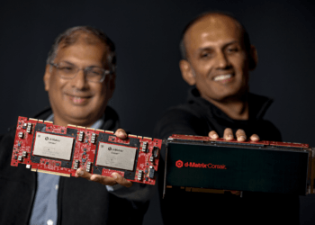
“Surrounded by established companies and innovative startups, the CHIPS for America Design and Collaboration Facility in Sunnyvale will enable NSTC members to address some of the most complex challenges in the semiconductor industry,” said Deirdre Hanford, CEO of Natcast.

  • Natcast is a purpose-built, non-profit entity designated by the U.S. Department of Commerce to operate the National Semiconductor Technology Center (NSTC), established under the CHIPS and Science Act. As a public-private consortium, the NSTC brings together government, industry, and academia to advance semiconductor research and development in the United States. Natcast’s mission is to serve as the focal point for research and engineering throughout the semiconductor ecosystem, advancing and enabling disruptive innovation to provide U.S. leadership in the industries of the future. 
ShareTweetShareSummarizeSummarize
Previous Post

Albany NY to Host CHIPS for America EUV Accelerator

Next Post

Huawei’s F5.5G Optical Network Strategy for Enhanced AI Connectivity

Jim Carroll

Jim Carroll

Editor and Publisher, Converge! Network Digest, Optical Networks Daily - Covering the full stack of network convergence from Silicon Valley

Related Posts

Optical

Colt and Ciena Achieve 800GbE Quantum-Safe Across the Atlantic

June 10, 2026
Semiconductors

Broadcom Targets 20 GW of AI Compute Capacity with $35B Financing

June 9, 2026
AI Infrastructure

Hut 8 Secures $4.25B Investment-Grade Financing for 352 MW Campus

June 9, 2026
AI Infrastructure

Crusoe Nears 5 GW of Contracted AI Infrastructure Capacity

June 9, 2026
All

Arista Unveils 1.6T Ethernet Portfolio for Rack-Scale AI Fabrics

June 9, 2026
Data Centers

d-Matrix Ramps Corsair AI Inference Platform

June 9, 2026
Next Post

Huawei’s F5.5G Optical Network Strategy for Enhanced AI Connectivity

Categories

  • 5G / 6G / Wi-Fi
  • AI Infrastructure
  • All
  • Automotive Networking
  • Blueprints
  • Clouds and Carriers
  • Data Centers
  • Enterprise
  • Explainer
  • Feature
  • Financials
  • Last Mile / Middle Mile
  • Legal / Regulatory
  • Optical
  • Quantum
  • Research
  • Security
  • Semiconductors
  • Space
  • Start-ups
  • Subsea
  • Sustainability
  • Video
  • Webinars

Archives

Tags

5G All AT&T Australia AWS Blueprint columns BroadbandWireless Broadcom China Ciena Cisco Data Centers Dell'Oro Ericsson FCC Financial Financials Huawei Infinera Intel Japan Juniper Last Mile Last Mille LTE Mergers and Acquisitions Mobile NFV Nokia Optical Packet Systems PacketVoice People Regulatory Satellite SDN Service Providers Silicon Silicon Valley StandardsWatch Storage TTP UK Verizon Wi-Fi
Converge Digest

A private dossier for networking and telecoms

Follow Us

  • Home
  • About
  • Events Calendar
  • Blueprint Guidelines
  • Privacy Policy
  • Manage Email Delivery
  • NextGenInfra.io

© 2026 Converge Digest - A private dossier for networking and telecoms.

No Result
View All Result
  • Home
  • About
  • Events Calendar
  • Blueprint Guidelines
  • Privacy Policy
  • Manage Email Delivery
  • NextGenInfra.io

© 2026 Converge Digest - A private dossier for networking and telecoms.

This website uses cookies. By continuing to use this website you are giving consent to cookies being used. Visit our Privacy and Cookie Policy.
Go to mobile version