• Home
  • About
  • Events Calendar
  • Blueprint Guidelines
  • Privacy Policy
  • Manage Email Delivery
  • NextGenInfra.io
  • buzzwords
  • Archives
  • Milestones
  • On This Day
  • Video Search
Converge Digest
Tuesday, July 14, 2026
  • Home
  • About
  • Events Calendar
  • Blueprint Guidelines
  • Privacy Policy
  • Manage Email Delivery
  • NextGenInfra.io
  • buzzwords
  • Archives
  • Milestones
  • On This Day
  • Video Search
No Result
View All Result
Converge Digest
No Result
View All Result

Home » EVG and Teramount target wafer-level silicon photonics packaging

EVG and Teramount target wafer-level silicon photonics packaging

March 1, 2022
in All, Silicon Photonics
A A

EV Group (EVG), a leading supplier of wafer bonding and lithography equipment for the MEMS, nanotechnology and semiconductor markets, announced a collaboration with Teramount on implementing wafer-level optics.

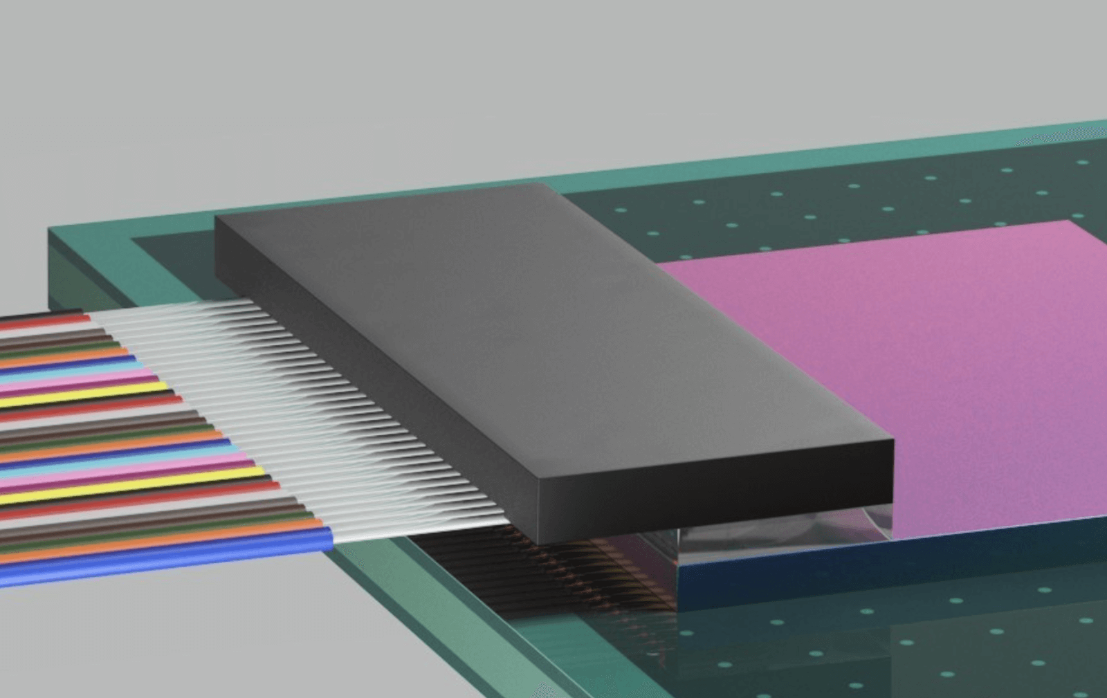
The collaboration will leverage EVG’s nanoimprint lithography (NIL) technology, expertise and services with Teramount’s PhotonicPlug technology.

Under this collaboration, standard CMOS wafers that implement silicon photonics chips will be post processed using EVG’s NIL technology to implement optical elements such as mirrors and lenses for Teramount’s unique “self-aligning optics”. This enables flexible beam extraction from the chips and easy connection to a large number of optical fibers. Furthermore, it enables wafer-level optical inspection capabilities for enhancing silicon photonics wafer manufacturing.

The collaboration is being carried out within EVG’s NILPhotonics Competence Center at its headquarters in St. Florian, Austria. The NILPhotonics Competence Center provides an open access innovation incubator for customers and partners across the NIL supply chain to collaborate to shorten development cycles and time to market for innovative photonic devices and applications. Through the collaboration with Teramount, EVG provides process development and production services, as well as expertise in both CMOS and photonics manufacturing, thus accelerating the commercialization of Teramount’s PhotonicPlug technology.

“Our joint work with EVG has been very successful in producing this innovative synergy between wafer-level optics and silicon photonics wafer manufacturing,” said Hesham Taha, CEO of Teramount. “By offering this capability to the industry, Teramount solves one of the major hurdles to further adoption of optical connectivity, which is critical for so many applications that require high-speed data transfers and low power consumption.”

“Teramount’s PhotonicPlug silicon photonics packaging technology is a truly novel approach to improving optical performance, and we are excited to be a partner in helping to bring it to the market,” stated Markus Wimplinger, Corporate Technology Development and IP Director at EV Group. “This is just the latest example of innovative technology developed with the support of EVG’s process and equipment know-how through our NILPhotonics Competence Center, where we help our partners and customers turn new ideas into innovative products.”


http://www.EVGroup.com

http://www.teramount.com

Tags: #OFC22Blueprint columns
ShareTweetShareSummarizeSummarize
Previous Post

Nokia and AT&T target 5G uplink with distributed massive MIMO

Next Post

Ericsson demos 5G Dynamic Radio Resource Partitioning

Staff

Staff

Related Posts

Blueprints

Blueprint: Brazil looks to municipal Wi-Fi 6E

February 21, 2023
All

Blueprint: Building wholesale networks with OTN

December 20, 2022
All

Oracle opens cloud region in Chicago

December 20, 2022
All

BT trials C-RAN in Leeds

December 19, 2022
All

T-Mobile builds cloud native 5G converged core with Cisco

December 15, 2022
All

Meta halts data center expansion construction in Denmark

December 15, 2022
Next Post

Ericsson demos 5G Dynamic Radio Resource Partitioning

Please login to join discussion

Categories

  • 5G / 6G / Wi-Fi
  • AI Infrastructure
  • All
  • Automotive Networking
  • Blueprints
  • Clouds and Carriers
  • Corporate Strategies
  • CPO
  • Data Centers
  • Enterprise
  • Explainer
  • Feature
  • Hot Start-ups
  • Last Mile / Middle Mile
  • Legal / Regulatory
  • Optical
  • Optical I/O
  • Pluggable Optics
  • Quantum
  • Research
  • Security
  • Semiconductors
  • Silicon Photonics
  • Space Networking & Orbital Data Centers
  • Subsea
  • Sustainability
  • Video
  • Webinars
Converge Digest

A private dossier for networking and telecoms

Follow Us

  • Home
  • About
  • Events Calendar
  • Blueprint Guidelines
  • Privacy Policy
  • Manage Email Delivery
  • NextGenInfra.io
  • buzzwords
  • Archives
  • Milestones
  • On This Day
  • Video Search

© 2026 Converge Digest - A private dossier for networking and telecoms.

No Result
View All Result
  • Home
  • About
  • Events Calendar
  • Blueprint Guidelines
  • Privacy Policy
  • Manage Email Delivery
  • NextGenInfra.io
  • buzzwords
  • Archives
  • Milestones
  • On This Day
  • Video Search

© 2026 Converge Digest - A private dossier for networking and telecoms.

This website uses cookies. By continuing to use this website you are giving consent to cookies being used. Visit our Privacy and Cookie Policy.
Go to mobile version