HyperLight closed an $80 million Series C financing round led by MediaTek to accelerate deployment of its thin-film lithium niobate photonics platform for AI infrastructure. The round includes UMC Capital, Jabil, Foxconn, EDBI, CDIB-TEN Capital, Qatar Investment Authority, and strategic investors from silicon IC and networking companies.
The Cambridge, Massachusetts company will use the funding to expand manufacturing capacity, accelerate customer qualification, scale its TFLN Chiplet Platform, and deepen partnerships across foundry, semiconductor, networking, and systems integration domains. HyperLight recently announced a strategic manufacturing partnership with UMC and Wavetek for high-volume foundry production on 6-inch and 8-inch wafers.
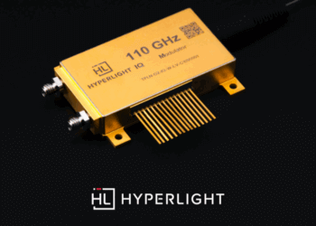
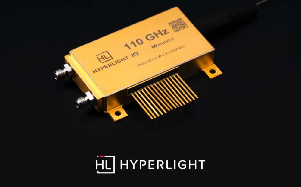
HyperLight’s TFLN Chiplet Platform targets short-reach IMDD data center pluggables, coherent datacom and telecom modules, and co-packaged optics. The platform supports 200G-per-lane operation, while 400G-per-lane solutions are now sampling. HyperLight positions TFLN as a path to lower drive voltage, high modulation bandwidth, and lower optical loss as AI networks move toward 3.2T and beyond.
• Series C: $80 million
• Lead investor: MediaTek
• Other investors: UMC Capital, Jabil, Foxconn, EDBI, CDIB-TEN Capital, QIA, and strategic silicon/networking investors
• Existing backers: Summit Partners, The Engine, Foothill Ventures, and Xora Innovation
• Technology: thin-film lithium niobate photonics
• Target markets: AI data centers, datacom, telecom, metro networks, and CPO
• Manufacturing focus: 6-inch and 8-inch TFLN wafer production
• Product status: 200G-per-lane supported; 400G-per-lane sampling
“This financing is about more than capital — it is about ecosystem alignment,” said Mian Zhang, CEO of HyperLight. “AI infrastructure requires optical interconnects that can deliver higher bandwidth, lower power, and manufacturing scale across pluggable optics and co-packaged optics.”
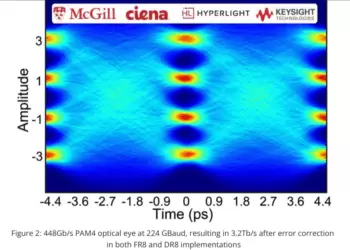
🌐 Analysis: HyperLight’s Series C links financial backing with a manufacturing and supply-chain strategy for TFLN photonics. Converge Digest previously covered HyperLight’s TFLN Chiplet Platform launch in March 2025, its 3.2Tbps O-band IMDD demonstration with Ciena and McGill in April 2025, and earlier TFLN modulator work showing sub-volt drive voltages and >100 GHz bandwidth. The new round moves the company’s narrative from device performance toward ecosystem qualification, foundry capacity, EMS alignment, and customer adoption for AI optical interconnects.
The investor mix matters. MediaTek brings silicon IC scale, UMC Capital connects to foundry manufacturing, Jabil and Foxconn connect to high-volume electronics manufacturing, and QIA/EDBI/CDIB-TEN add global infrastructure and Asia supply-chain capital. For AI networks, the timing aligns with the shift toward 200G and 400G electrical/optical lanes, 3.2T pluggables, and CPO roadmaps where modulator bandwidth, voltage, insertion loss, and manufacturability directly affect power and packaging budgets.
| Profile: HyperLight | |
| HQ | Cambridge, Massachusetts |
| CEO | Mian Zhang |
| Core technology | Thin-film lithium niobate photonics for high-bandwidth, low-voltage optical modulation |
| Platform | TFLN Chiplet Platform for IMDD pluggables, coherent optics, telecom modules, and CPO |
| Latest funding | $80 million Series C led by MediaTek |
| Strategic investors | MediaTek, UMC Capital, Jabil, Foxconn, EDBI, CDIB-TEN Capital, QIA, and others |
| Manufacturing | UMC/Wavetek partnership for 6-inch and 8-inch TFLN wafer production |
| Recent milestones | TFLN Chiplet Platform launch; 3.2Tbps O-band IMDD demo with Ciena and McGill; 400G-per-lane sampling |
| Understanding Thin-Film Lithium Niobate (TFLN) | |
| What is TFLN? | Thin-Film Lithium Niobate (TFLN) is an integrated photonics platform that bonds a sub-micron single-crystal lithium niobate layer onto a silicon or quartz substrate. It marries the exceptional electro-optic performance of traditional bulk LN with the high-density wafer-scale manufacturing of silicon photonics. |
| Physics & Edge | By tightly confining light within nanoscale waveguides, TFLN maximizes the linear electro-optic (Pockels) effect. This yields ultra-high modulation bandwidth, sub-1V drive voltages ($V_\pi$), and near-zero chirp—allowing direct driving by DSPs or switch ASICs without power-hungry analog drivers. |
| AI Cluster Role | Next-gen GPU clusters require massive, low-latency east-west bandwidth. As electrical interconnects hit physical limits at 224G SerDes, TFLN enables the transition to 1.6T and 3.2T optical links, significantly slashing power consumption ($pJ/bit$) and thermal overhead at the optical interface. |
| Evolution | Bulk lithium niobate modulators have been the workhorse of long-haul telecom and transoceanic subsea networks for decades due to their unmatched reliability. TFLN miniaturizes this proven material by orders of magnitude, moving it from bulky discrete components into chip-scale photonic integrated circuits (PICs). |
| Form Factors | Crucial for 200G-per-lane and 400G-per-lane optical paths. It is actively being deployed in 800G/1.6T OSFP/QSFP-DD pluggable transceivers, coherent metro/long-haul modules, Linear Drive Opticals (LPO/LRO), and upcoming Co-Packaged Optics (CPO) architectures. |
| The Landscape | Competes with and complements traditional Silicon Photonics (SiPh), Indium Phosphide (InP), and Barium Titanate (BTO). The prevailing market trend favors heterogeneous integration—using SiPh for complex routing/multiplexing and bonding TFLN chiplets specifically for ultra-fast modulation. |
| Scaling Trend | Transitioning rapidly from boutique fabrication to commercial 6-inch and 8-inch CMOS foundries. Standardized dry-etching techniques and automated PIC packaging ecosystems are lowering per-port costs, clearing the path for hyperscale data center volumes. |
🌐 We’re tracking the latest developments in optical networking. Follow our ongoing coverage at: https://convergedigest.com/category/optical/