Kyocera Corporation introduced a new multilayer ceramic core substrate targeting advanced semiconductor packaging for AI processors and switch ASICs, addressing scaling challenges in next-generation data center architectures. The company will showcase the technology at the ECTC 2026, scheduled for May 26–29 in Orlando, Florida.
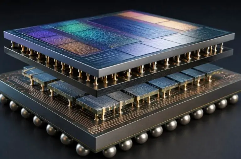
The substrate leverages Kyocera’s Fine Ceramic materials to deliver higher rigidity and improved dimensional stability compared to conventional organic core substrates. This approach directly targets package warpage—one of the primary constraints in large, high-performance semiconductor packages—while enabling thinner substrates and improved electrical performance. The company positions the technology for use in xPU-class devices, including CPUs and GPUs, as well as high-bandwidth switch ASICs used in AI clusters.
Kyocera said the multilayer ceramic structure enables finer wiring density through advanced via formation techniques. Unlike drilled vias in organic substrates, ceramic vias are formed during the pre-sintering phase, allowing smaller diameters and tighter pitch. The company also provides simulation capabilities during the design phase, including thermal, electrical, and warpage modeling, to support co-optimization of packaging and device performance for 2.5D integration architectures.
- Targets advanced packaging for xPUs (CPUs, GPUs) and switch ASICs used in AI data centers
- Multilayer ceramic core reduces warpage compared to organic substrates, improving reliability
- Enables high-density, three-dimensional wiring for greater circuit miniaturization
- Supports 2.5D packaging architectures with improved dimensional stability
- Offers simulation tools (thermal, electrical, warpage) during design phase
- Designed for large, high-performance packages required by AI and HPC workloads
“Kyocera remains committed to developing new packaging materials and technologies that meet evolving customer needs in the semiconductor industry.”
🌐 Analysis: Kyocera’s move reflects a broader industry push to overcome substrate-level limitations as AI accelerators scale in size, power, and interconnect density. Warpage and routing density have emerged as critical bottlenecks in 2.5D and chiplet-based designs, particularly for high-bandwidth memory (HBM) integration and large reticle-sized packages.
Ceramic substrates offer clear mechanical and dimensional advantages, but they face trade-offs in cost, manufacturability, and ecosystem maturity compared to organic substrates and silicon interposers. Competitors across the advanced packaging ecosystem—including companies working on glass substrates, silicon interposers, and advanced organic laminates—are pursuing parallel approaches. The adoption trajectory will depend on whether ceramic substrates can scale economically while meeting the stringent yield and integration requirements of hyperscale AI deployments.