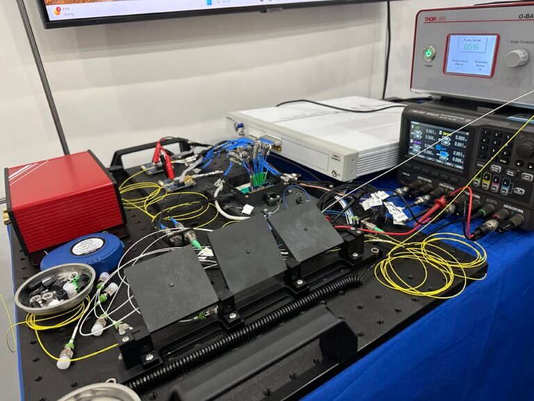
Lumentum used OFC 2026 to showcase a new optical interconnect platform for AI scale-up networks based on 1060nm VCSEL technology. The company said the solution is designed for next-generation rack-level architectures, where bandwidth, power, and integration constraints are becoming more severe as AI systems scale. The demonstration points to a growing effort to bring optical interconnects deeper into the rack and closer to the ASIC for short-reach scale-up links.
The demonstration featured a high-density multimode 1060nm VCSEL array co-packaged with a host ASIC in a host evaluation system. Lumentum said the platform targets “slow and wide” scale-up protocols such as UCIe and PCIe and is implemented in a fan-out wafer-level package using standard semiconductor packaging flows and advanced multimode fiber connectivity. The company said the 1060nm VCSELs and photodetectors are integrated in a two-dimensional monolithic array with backside lens technology to support optical alignment and signal integrity.
Lumentum also said the array architecture supports channel sparing for improved system reliability and is designed for demanding environments with operating temperatures exceeding 150°C. The company said its 1060nm VCSEL platform builds on an ultra-high-volume 3D sensing manufacturing base that has shipped more than 10 billion emitters. Lumentum added that, compared with conventional 850nm datacom VCSELs, its 1060nm devices offer improved speed capability, stronger high-temperature performance, and longer-term reliability, while also providing a supply-chain alternative to silicon photonics and InP laser-based approaches.
- Demonstration centered on a 1060nm VCSEL optical scale-up platform for AI rack-level architectures
- Targets UCIe and PCIe scale-up protocols
- Uses a high-density multimode VCSEL array co-packaged with a host ASIC
- Implemented in fan-out wafer-level packaging
- Combines standard semiconductor packaging flows with advanced multimode fiber connectivity
- Integrates VCSELs and photodetectors in a 2D monolithic array with backside lens technology
- Supports channel sparing for enhanced reliability
- Designed for operating temperatures above 150°C (302°F)
- Built on Lumentum’s 3D sensing manufacturing base with more than 10 billion emitters shipped
- Positions VCSEL technology as an alternative supply path to silicon photonics and InP laser architectures
“AI infrastructure is pushing the limits of conventional electrical interconnects,” said Matt Sysak, Chief Technology Officer at Lumentum. “Our 1060nm VCSEL scale-up platform optically enables ASICs with high shoreline bandwidth density, strong signal integrity, and thermal resilience, while providing a differentiated and highly reliable alternative to traditional silicon photonics-based approaches.”
🌐 Analysis: Lumentum’s announcement highlights a broader architecture question in AI systems: whether short-reach scale-up links inside racks and tightly integrated compute domains will continue to rely mainly on copper, or increasingly shift toward optical approaches as bandwidth density and thermal limits tighten. In that context, the company is making the case that VCSEL-based optics could play a role alongside silicon photonics and InP-based designs for specific short-reach interconnect scenarios.