nEye.ai, a start-up based in Santa Clara, California, raised $80 million in Series C funding to scale its optical circuit switching technology for AI infrastructure, with the round led by Sutter Hill Ventures and participation from CapitalG, M12, and Socratic Partners. The Santa Clara-based startup now reports total funding of $152 million as it accelerates development and production of its Optical Circuit Switch (OCS) platform. The investment comes as hyperscale AI data centers push toward more flexible, composable architectures to support increasingly large training and inference workloads.
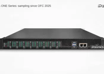
The company’s OCS technology integrates silicon photonics, MEMS, and CMOS into a single chip, enabling high-density, low-power optical switching. Unlike traditional mechanical optical switches, nEye’s wafer-scale, foundry-compatible approach targets improved scalability and cost efficiency. The architecture supports dynamic pooling of compute, memory, and storage resources, aligning with emerging “scale-up, scale-out, and scale-across” AI data center designs.
nEye plans to use the funding to expand high-volume manufacturing and meet performance requirements from hyperscale customers. As part of the financing, Stefan Dyckerhoff of Sutter Hill Ventures joins the board. The company positions its “OCS-on-a-chip” approach as a key enabler for next-generation AI fabrics, where bandwidth density, latency, and power efficiency remain critical constraints.
- $80 million Series C led by Sutter Hill Ventures; total funding reaches $152 million
- Investors include CapitalG (Alphabet), M12 (Microsoft), Socratic Partners, and Micron Technology
- Focus on Optical Circuit Switching (OCS) for AI data center interconnects
- Integration of silicon photonics, MEMS, and CMOS into a single chip
- Targets composable infrastructure with dynamic resource pooling across CPUs, GPUs, and memory
- Emphasis on wafer-scale, foundry-compatible manufacturing for cost and scalability advantages
- Addresses power and density constraints in hyperscale AI environments
“While this milestone validates our technology, our focus now shifts to scaling our foundry-based manufacturing and meeting the rigorous performance standards our customers demand,” said Ashish Vengsarkar, CEO of nEye.ai.
🌐 Analysis: nEye’s approach reflects a broader industry shift toward optical switching as a complement—or alternative—to electrical packet switching in AI clusters, particularly as east-west traffic intensifies. Startups and incumbents alike, including developments in silicon photonics fabrics and co-packaged optics, continue to explore similar architectures to reduce power consumption and improve utilization in large-scale GPU deployments.
nEye.ai was founded by CEO Ashish Vengsarkar alongside Dr. Ming C. Wu and Dr. Tae Joon Seok, combining deep expertise across optical networking, silicon photonics, and MEMS. Vengsarkar brings more than three decades of industry experience, including leadership roles at Google building optical networks and founding startups such as Photuris and Nistica, with over $100 million raised across multiple venture rounds and several successful exits. Dr. Wu, a Nortel Distinguished Professor at UC Berkeley, is widely recognized for pioneering work in silicon photonics, MEMS, and optofluidics, and previously co-founded Berkeley Lights and Optical Micro-Machines. Dr. Seok, an expert in integrated photonics and optoelectronics, has held academic and research roles at GIST and UC Berkeley, contributing more than 40 technical publications and earning industry recognition for innovation in optical technologies. Together, the founding team blends academic leadership with startup execution and large-scale networking experience to advance nEye’s OCS-on-chip architecture for AI data centers.
| Open Compute Project (OCP) – Optical Circuit Switching (OCS) Initiative for AI Infrastructure | |
|---|---|
 | |
| Initiative | OCP Optical Circuit Switching (OCS) Project |
| Objective | Define open architectures for dynamic, high-bandwidth optical switching in AI and hyperscale data centers |
| Primary Use Case | AI training clusters requiring reconfigurable, low-latency interconnects across GPUs, CPUs, and memory pools |
| Key Concept | Circuit-based optical paths that can be dynamically reconfigured to optimize workload placement and resource utilization |
| Architecture Model | Complementary to packet switching; enables scale-up, scale-out, and scale-across topologies |
| Technology Components | Silicon photonics, MEMS-based switching, integrated optics, and high-density fiber interconnects |
| Performance Goals | Ultra-low latency, high radix switching, reduced power consumption, and improved bandwidth utilization |
| Industry Drivers | Explosive east-west traffic in AI clusters, GPU underutilization, and power constraints in hyperscale facilities |
| Key Contributors | Hyperscalers, optical component vendors, and emerging OCS ecosystem participants |