• Home
  • About
  • Events Calendar
  • Blueprint Guidelines
  • Privacy Policy
  • Manage Email Delivery
  • NextGenInfra.io
  • buzzwords
  • Archives
  • Milestones
  • On This Day
  • Video Search
Converge Digest
Tuesday, July 14, 2026
  • Home
  • About
  • Events Calendar
  • Blueprint Guidelines
  • Privacy Policy
  • Manage Email Delivery
  • NextGenInfra.io
  • buzzwords
  • Archives
  • Milestones
  • On This Day
  • Video Search
No Result
View All Result
Converge Digest
No Result
View All Result

Home » NVIDIA opens its NVLink die-to-die and chip-to-chip

NVIDIA opens its NVLink die-to-die and chip-to-chip

March 22, 2022
in All
A A

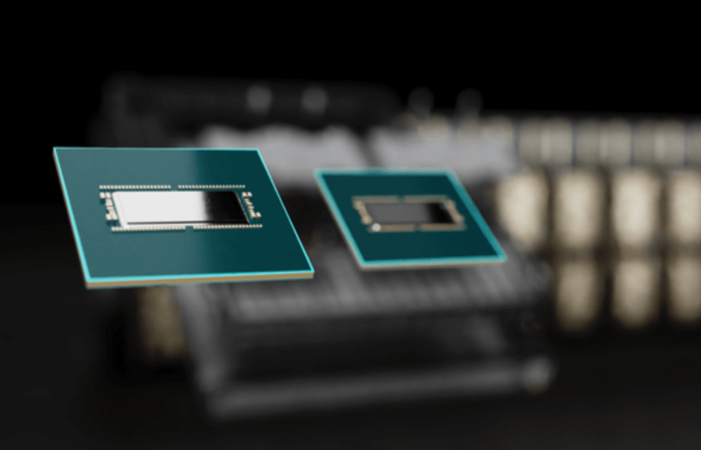
NVIDIA will expand the use of its NVLink chip-to-chip and die-to-die interconnect technology in its GPUs, CPUs, DPUs, NICs and SOCs. The company also plans to open the technolgy to other for for custom chip and chiplet integrations. 

NVIDIA NVLink-C2C is built on top of NVIDIA’s world-class SERDES and LINK design technology, and it is extensible from PCB-level integrations and multichip modules to silicon interposer and wafer-level connections, delivering extremely high bandwidth while optimizing for energy and die area efficiency.

In addition to NVLink-C2C, NVIDIA will also support the developing Universal Chiplet Interconnect Express (UCIe) standard. Custom silicon integration with NVIDIA chips can either use the UCIe standard or NVLink-C2C, which is optimized for lower latency, higher bandwidth and greater power efficiency.

Some of NVLink-C2C’s key features include:

● High Bandwidth – supporting high-bandwidth coherent data transfers between processors and accelerators

● Low Latency – supporting atomics between processors and accelerators to perform fast synchronization and high-frequency updates to shared data

● Low Power and High Density – using advanced packaging, it is 25x more energy efficient and 90x more area-efficient than PCIe Gen 5 on NVIDIA chips

● Industry-Standard Support – works with Arm’s AMBA CHI or CXL industry-standard protocols for interoperability between devices

“Chiplets and heterogeneous computing are necessary to counter the slowing of Moore’s law,” said Ian Buck, vice president of Hyperscale Computing at NVIDIA. “We’ve used our world-class expertise in high-speed interconnects to build uniform, open technology that will help our GPUs, DPUs, NICs, CPUs and SoCs create a new class of integrated products 

NVIDIA estimates that its NVLink-C2C interconnect could deliver up to 25x more energy efficiency and be 90x more area-efficient than PCIe Gen 5 on NVIDIA chips and enable coherent interconnect bandwidth of 900 Gbps or higher.

“As the future of CPU design is increasingly accelerated and multichip, it is critical to support chiplet-based SoCs across the ecosystem,” said Chris Bergey, senior vice president and general manager of the Infrastructure Line of Business at Arm. “Arm is supporting a broad set of connectivity standards and designing our AMBA CHI protocol to support these future technologies, including collaborating with NVIDIA on NVLink-C2C to address use cases like coherent connectivity between CPUs, GPUs and DPUs.”

https://www.nvidia-press.com/f/preview/27653

Tags: Blueprint columnsNvidia
ShareTweetShareSummarizeSummarize
Previous Post

Ericsson intros Local Packet Gateway for enterprises

Next Post

NVIDIA unveils 51.2T Spectrum-4 switch ASIC

Staff

Staff

Related Posts

5G / 6G / Wi-Fi

NVIDIA Pushes Telecom AI Toward Autonomous Operations at DTW Ignite 2026

June 23, 2026
All

Groq Raises $650 Million to Expand AI Inference Cloud

June 22, 2026
AI Infrastructure

NVIDIA: Europe Unveils Record 35 AI Supercomputers

June 22, 2026
AI Infrastructure

NVIDIA Expands Korea AI Push

June 7, 2026
Vera Rubin Cluster
AI Infrastructure

NVIDIA Vera Rubin Enters Full Production 

May 31, 2026
All

NVIDIA Adds In-Silicon Security to Vera BlueField-4 STX 

May 31, 2026
Next Post

NVIDIA unveils 51.2T Spectrum-4 switch ASIC

Please login to join discussion

Categories

  • 5G / 6G / Wi-Fi
  • AI Infrastructure
  • All
  • Automotive Networking
  • Blueprints
  • Clouds and Carriers
  • Corporate Strategies
  • CPO
  • Data Centers
  • Enterprise
  • Explainer
  • Feature
  • Hot Start-ups
  • Last Mile / Middle Mile
  • Legal / Regulatory
  • Optical
  • Optical I/O
  • Pluggable Optics
  • Quantum
  • Research
  • Security
  • Semiconductors
  • Silicon Photonics
  • Space Networking & Orbital Data Centers
  • Subsea
  • Sustainability
  • Video
  • Webinars
Converge Digest

A private dossier for networking and telecoms

Follow Us

  • Home
  • About
  • Events Calendar
  • Blueprint Guidelines
  • Privacy Policy
  • Manage Email Delivery
  • NextGenInfra.io
  • buzzwords
  • Archives
  • Milestones
  • On This Day
  • Video Search

© 2026 Converge Digest - A private dossier for networking and telecoms.

No Result
View All Result
  • Home
  • About
  • Events Calendar
  • Blueprint Guidelines
  • Privacy Policy
  • Manage Email Delivery
  • NextGenInfra.io
  • buzzwords
  • Archives
  • Milestones
  • On This Day
  • Video Search

© 2026 Converge Digest - A private dossier for networking and telecoms.

This website uses cookies. By continuing to use this website you are giving consent to cookies being used. Visit our Privacy and Cookie Policy.
Go to mobile version