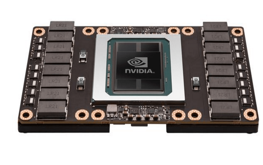
NVIDIA unveiled its most advanced accelerator to date — the Tesla P100 — based on Pascal architecture and composed of an array of Graphics Processing Clusters (GPCs), Streaming Multiprocessors (SMs), and memory controllers. The Tesla P100, which is implemented in 16nm FinFET on a massive 610mm2die, enables a new class of servers that can deliver the performance of hundreds of CPU server nodes.


NVIDIA said its accelerator brings five breakthroughs:
- NVIDIA Pascal architecture for exponential performance leap — a Pascal-based Tesla P100 solution delivers over a 12x increase in neural network training performance compared with a previous-generation NVIDIA Maxwell-based solution.
- NVIDIA NVLink for maximum application scalability — The NVIDIA NVLink high-speed GPU interconnect scales applications across multiple GPUs, delivering a 5x acceleration in bandwidth compared to today’s best-in-class solution. Up to eight Tesla P100 GPUs can be interconnected with NVLink to maximize application performance in a single node, and IBM has implemented NVLink on its POWER8 CPUs for fast CPU-to-GPU communication.
- 16nm FinFET for unprecedented energy efficiency — with 15.3 billion transistors built on 16 nanometer FinFET fabrication technology, the Pascal GPU is the world’s largest FinFET chip ever built.
- CoWoS with HBM2 for big data workloads — the Pascal architecture unifies processor and data into a single package to deliver unprecedented compute efficiency. An innovative approach to memory design, Chip on Wafer on Substrate (CoWoS) with HBM2, provides a 3x boost in memory bandwidth performance, or 720GB/sec, compared to the Maxwell architecture.
- New AI algorithms for peak performance — new half-precision instructions deliver more than 21 teraflops of peak performance for deep learning.
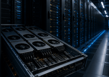
 At its GPU Technology conference in San Jose, Nvidia also unveiled its DGX-1 Deep Learning supercomputer. It is a turnkey system that integrates eight Tesla P100 GPU accelerators, delivering the equivalent throughput of 250 x86 servers.
“Artificial intelligence is the most far-reaching technological advancement in our lifetime,” said Jen-Hsun Huang, CEO and co-founder of NVIDIA. “It changes every industry, every company, everything. It will open up markets to benefit everyone. Data scientists and AI researchers today spend far too much time on home-brewed high performance computing solutions. The DGX-1 is easy to deploy and was created for one purpose: to unlock the powers of superhuman capabilities and apply them to problems that were once unsolvable.”
“NVIDIA GPU is accelerating progress in AI. As neural nets become larger and larger, we not only need faster GPUs with larger and faster memory, but also much faster GPU-to-GPU communication, as well as hardware that can take advantage of reduced-precision arithmetic. This is precisely what Pascal delivers,” said Yann LeCun, director of AI Research at Facebook.