• Home
  • About
  • Events Calendar
  • Blueprint Guidelines
  • Privacy Policy
  • Manage Email Delivery
  • NextGenInfra.io
  • buzzwords
  • Archives
  • Milestones
  • On This Day
  • Video Search
Converge Digest
Tuesday, July 14, 2026
  • Home
  • About
  • Events Calendar
  • Blueprint Guidelines
  • Privacy Policy
  • Manage Email Delivery
  • NextGenInfra.io
  • buzzwords
  • Archives
  • Milestones
  • On This Day
  • Video Search
No Result
View All Result
Converge Digest
No Result
View All Result

Home » Samsung demos first MRAM based in-memory computing

Samsung demos first MRAM based in-memory computing

January 13, 2022
in All
A A

Samsung Electronics Co. announced the first demonstration of in-memory computing based on MRAM (Magnetoresistive Random Access Memory). 

In memory computing differs from standard computer architecture in that both data storage and data computing is performed in a memory network. Since this scheme can process a large amount of data stored within the memory network itself without having to move the data, and also because the data processing in the memory network is executed in a highly parallel manner, power consumption is substantially reduced. In-memory computing has thus emerged as one of the promising technologies to realize next-generation low-power AI semiconductor chips.

The research was led by Samsung Advanced Institute of Technology (SAIT) in close collaboration with Samsung Electronics Foundry Business and Semiconductor R&D Center. The first author of the paper, Dr. Seungchul Jung, Staff Researcher at SAIT, and the co-corresponding authors Dr. Donhee Ham, Fellow of SAIT and Professor of Harvard University, and Dr. Sang Joon Kim, Vice President of Technology at SAIT, spearheaded the research.

The Samsung Electronics researchers have provided a solution to this issue by an architectural innovation. Concretely, they succeeded in developing an MRAM array chip that demonstrates in-memory computing, by replacing the standard, ‘current-sum’ in-memory computing architecture with a new, ‘resistance sum’ in-memory computing architecture, which addresses the problem of small resistances of individual MRAM devices.

Samsung’s research team subsequently tested the performance of this MRAM in-memory computing chip by running it to perform AI computing. The chip achieved an accuracy of 98% in classification of hand-written digits and a 93% accuracy in detecting faces from scenes.

“In-memory computing draws similarity to the brain in the sense that in the brain, computing also occurs within the network of biological memories, or synapses, the points where neurons touch one another,” said Dr. Seungchul Jung, the first author of the paper. “In fact, while the computing performed by our MRAM network for now has a different purpose from the computing performed by the brain, such solid-state memory network may in the future be used as a platform to mimic the brain by modelling the brain’s synapse connectivity.”

https://research.samsung.com/news

Tags: Blueprint columnsSamsung
ShareTweetShareSummarizeSummarize
Previous Post

IDC: Cloud infrastructure spending accelerates

Next Post

Comcast tests 10G modem based on full Duplex DOCSIS 4.0

Staff

Staff

Related Posts

5G / 6G / Wi-Fi

Samsung AI RAN Optimizer Boosts KDDI 5G Throughput by Up to 52%

July 6, 2026
AI Infrastructure

South Korea Unveils National AI Infrastructure Strategy 

June 29, 2026
All

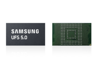
Samsung’s UFS 5.0 Doubles Storage Performance for AI Smartphones

June 26, 2026
5G / 6G / Wi-Fi

Broadcom and Samsung Link 5G Release 17 Modem with Wi-Fi 8

May 27, 2026
Enterprise

KKR Invests $820 Million in Samsung SDS

April 14, 2026
Space Networking & Orbital Data Centers

Keysight, Samsung Showcase NR-NTN LEO Mobility Testing 

February 5, 2026
Next Post

Comcast tests 10G modem based on full Duplex DOCSIS 4.0

Please login to join discussion

Categories

  • 5G / 6G / Wi-Fi
  • AI Infrastructure
  • All
  • Automotive Networking
  • Blueprints
  • Clouds and Carriers
  • Corporate Strategies
  • CPO
  • Data Centers
  • Enterprise
  • Explainer
  • Feature
  • Hot Start-ups
  • Last Mile / Middle Mile
  • Legal / Regulatory
  • Optical
  • Optical I/O
  • Pluggable Optics
  • Quantum
  • Research
  • Security
  • Semiconductors
  • Silicon Photonics
  • Space Networking & Orbital Data Centers
  • Subsea
  • Sustainability
  • Video
  • Webinars
Converge Digest

A private dossier for networking and telecoms

Follow Us

  • Home
  • About
  • Events Calendar
  • Blueprint Guidelines
  • Privacy Policy
  • Manage Email Delivery
  • NextGenInfra.io
  • buzzwords
  • Archives
  • Milestones
  • On This Day
  • Video Search

© 2026 Converge Digest - A private dossier for networking and telecoms.

No Result
View All Result
  • Home
  • About
  • Events Calendar
  • Blueprint Guidelines
  • Privacy Policy
  • Manage Email Delivery
  • NextGenInfra.io
  • buzzwords
  • Archives
  • Milestones
  • On This Day
  • Video Search

© 2026 Converge Digest - A private dossier for networking and telecoms.

This website uses cookies. By continuing to use this website you are giving consent to cookies being used. Visit our Privacy and Cookie Policy.
Go to mobile version