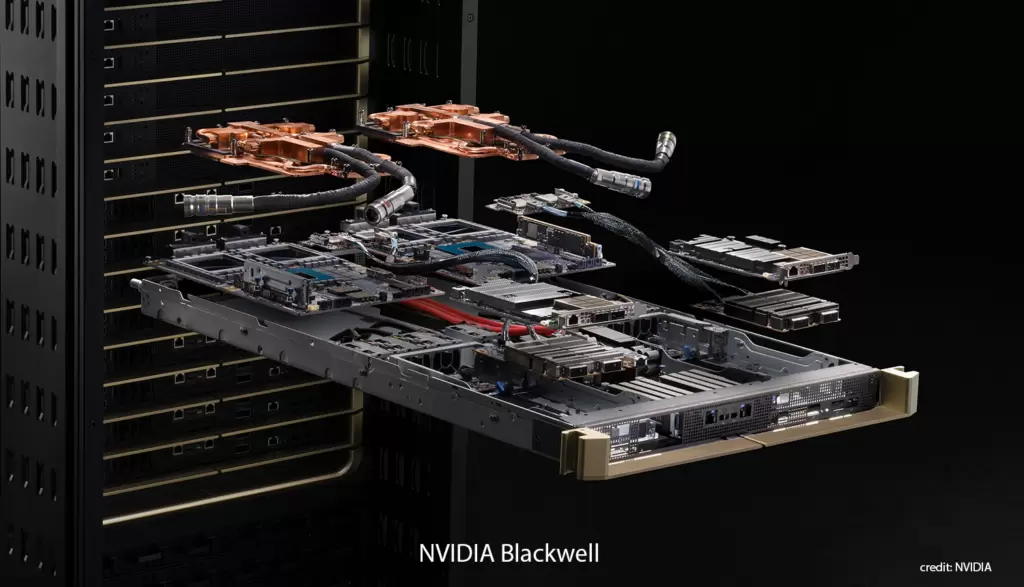
Ahead of the Hot Chips 2024 conference next week at Stanford University, NVIDIA highlighted the capabilities of Blackwell, its next flagship GPU. In a press briefing, NVIDIA execs shared photos of Blackwell up and running in an NVIDIA data center, emphasizing that Blackwell is a platform consisting of multiple chips integrated into a system-level solution optimized for real-time, large language model inferencing. Rapidly expanding performance requirements, as measured in user tokens per second, necessitate multiple GPUs, and soon multiple server nodes.
Achieving this performance requires a very powerful network connecting all of these components within the rack. Here, NVIDIA is pitching its NV Switch — basically the fabric that allows GPUs to talk to each other at a rate “much, much faster than any other interconnect” — one hop from one GPU to any other GPU initially at 900
gigabytes per second. With the new Blackwell NV Switch, NVIDIA is doubling the bandwidth to 1.8 terabytes per second. If you aggregate the bandwidth from 2 NVLink chips running at full speed, you get 14.4 terabytes per second of total switch capacity.
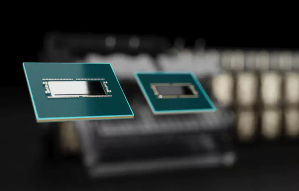
Key features of Blackwell NVLink Switch Chip
- 800 mm2 in TSMC 4NP
- Extends NVLink to 72 GPUs on GB200 NVL72
- 7.2 TB/s full all-to-all bidirectional BW over 72 ports
- SHARP In-Network Compute — 3.6 TFLOPS

Other topics that NVIDIA plans to highlight at Hot Chips include a liquid-cooled solution that integrates 72 Blackwell GPUs and 36 Grace CPUs, enabling significant advancements in power savings. Additionally, NVIDIA will discuss how hybrid liquid-cooling , including a warm water solution, are transforming data center infrastructure and how AI models are increasingly supporting the complex task of semiconductor design.
Key NVIDIA Topics at Hot Chips:
• Blackwell Platform: NVIDIA will discuss the integration of multiple technologies, including Blackwell GPUs, Grace CPUs, and NVLink, to advance AI and computing performance.
• Liquid Cooling: Introduction of liquid-cooled data center solutions that enhance energy efficiency and reduce operational costs.
• AI for Chip Design: NVIDIA will showcase AI agents that assist in processor design, improving productivity and design quality.
• Quasar Quantization System: An innovation to push the limits of AI computing with low-precision models while maintaining high accuracy.
• GB200 NVL72: A multi-node, liquid-cooled system that dramatically speeds up AI inference, supporting real-time operation of trillion-parameter models.
FROM OUR ARCHIVE
About NVIDIA’s NVLink: High-Speed GPU Interconnect Technology
NVLink is NVIDIA’s proprietary high-speed interconnect technology, designed to facilitate rapid data exchange between GPUs and other system components like CPUs and memory. It aims to surpass the limitations of traditional PCIe connections by offering increased bandwidth and reduced latency.
NVIDIA NVLink-C2C is built on top of NVIDIA’s world-class SERDES and LINK design technology, and it is extensible from PCB-level integrations and multichip modules to silicon interposer and wafer-level connections, delivering extremely high bandwidth while optimizing for energy and die area efficiency.
Key features:
- High bandwidth: Significantly faster than PCIe, with speeds exceeding 100 GB/s in some configurations.
- Scalability: Enables efficient multi-GPU setups for parallel processing in HPC environments.
- Unified memory: Allows direct memory access between GPUs, improving efficiency for large datasets.
- Low latency: Enhances performance for workloads requiring frequent inter-GPU communication.
- Advanced architecture support: Used in NVIDIA’s high-end GPU architectures for powerful computing systems.
NVLink has evolved through several generations, each offering improved performance:
- NVLink 1.0 (Pascal): 40 GB/s bidirectional bandwidth per link
- NVLink 2.0 (Volta): 50 GB/s per link
- NVLink 3.0 (Ampere): 100 GB/s per link
- NVLink 4.0 (Hopper): Up to 900 GB/s aggregate bandwidth in some configurations