Wolfspeed positions 300mm silicon carbide as a materials platform for next-generation AI and HPC packaging
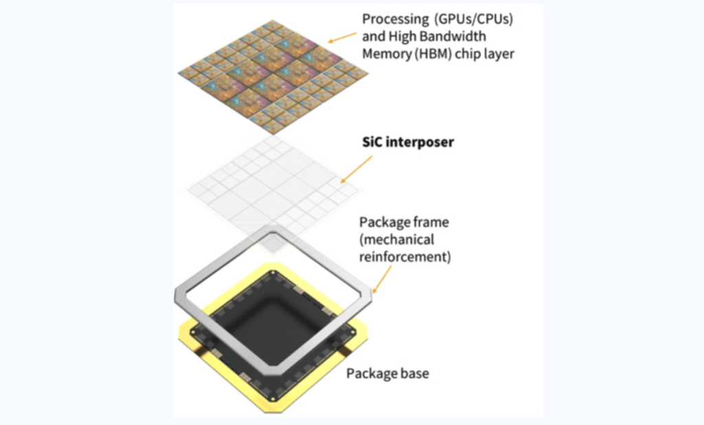
Wolfspeed outlined a new roadmap for using 300mm silicon carbide (SiC) substrates as a foundational materials platform for advanced heterogeneous packaging in AI and high-performance computing systems. The company said its patent-pending innovations could enable large interposer and heat-spreader structures capable of supporting the growing package sizes and power densities emerging in next-generation AI infrastructure.
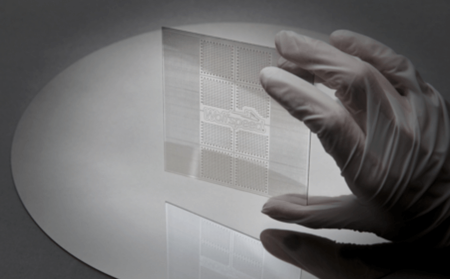
The concept builds on Wolfspeed’s January 2026 milestone of producing a single-crystal 300mm SiC wafer. The company now plans to explore how this wafer format can serve as the basis for advanced packaging components used in large heterogeneous compute modules that combine GPUs, CPUs, memory, and specialized accelerators. As AI clusters scale, semiconductor packages continue to grow in both physical size and integration complexity, placing increasing pressure on conventional silicon and organic substrate materials.
Wolfspeed said silicon carbide offers a combination of high thermal conductivity, mechanical strength, and favorable electrical properties that could help address thermal and reliability challenges in large AI processor packages. The company is working with foundries, OSATs, system architects, and research institutions to evaluate how hybrid silicon–SiC packaging architectures could be integrated into standard semiconductor manufacturing flows using existing 300mm infrastructure.
- Wolfspeed is exploring the use of 300mm silicon carbide substrates as a materials platform for AI and HPC heterogeneous packaging.
- The approach could enable large interposers and heat spreaders for multi-die compute modules used in advanced AI systems.
- Silicon carbide offers high thermal conductivity, strong mechanical stability, and favorable electrical characteristics compared with conventional materials.
- The 300mm wafer format aligns with existing semiconductor manufacturing infrastructure, supporting potential high-volume production.
- Wolfspeed is collaborating with foundries, OSAT providers, system architects, and research institutions to assess feasibility and reliability.
“Our 300mm silicon carbide platform is designed to align SiC’s material advantages with industry-standard manufacturing infrastructure and expand the solution space for next-generation AI and HPC packaging architectures,” said Elif Balkas, Chief Technology Officer at Wolfspeed.
🌐 Analysis
Advanced packaging has become a critical bottleneck for AI infrastructure as compute modules integrate ever larger numbers of chiplets, high-bandwidth memory stacks, and specialized accelerators. Materials capable of supporting higher thermal loads and larger interposer footprints are attracting attention across the semiconductor ecosystem as package sizes approach reticle limits and system power levels climb toward multi-kilowatt ranges.
Wolfspeed’s work positions silicon carbide—traditionally used in power electronics—as a potential materials platform for heterogeneous compute packaging. The effort aligns with broader industry exploration of alternative packaging substrates and interposer materials as companies such as NVIDIA, AMD, and hyperscale AI infrastructure providers continue pushing toward larger, higher-power multi-die AI processors.