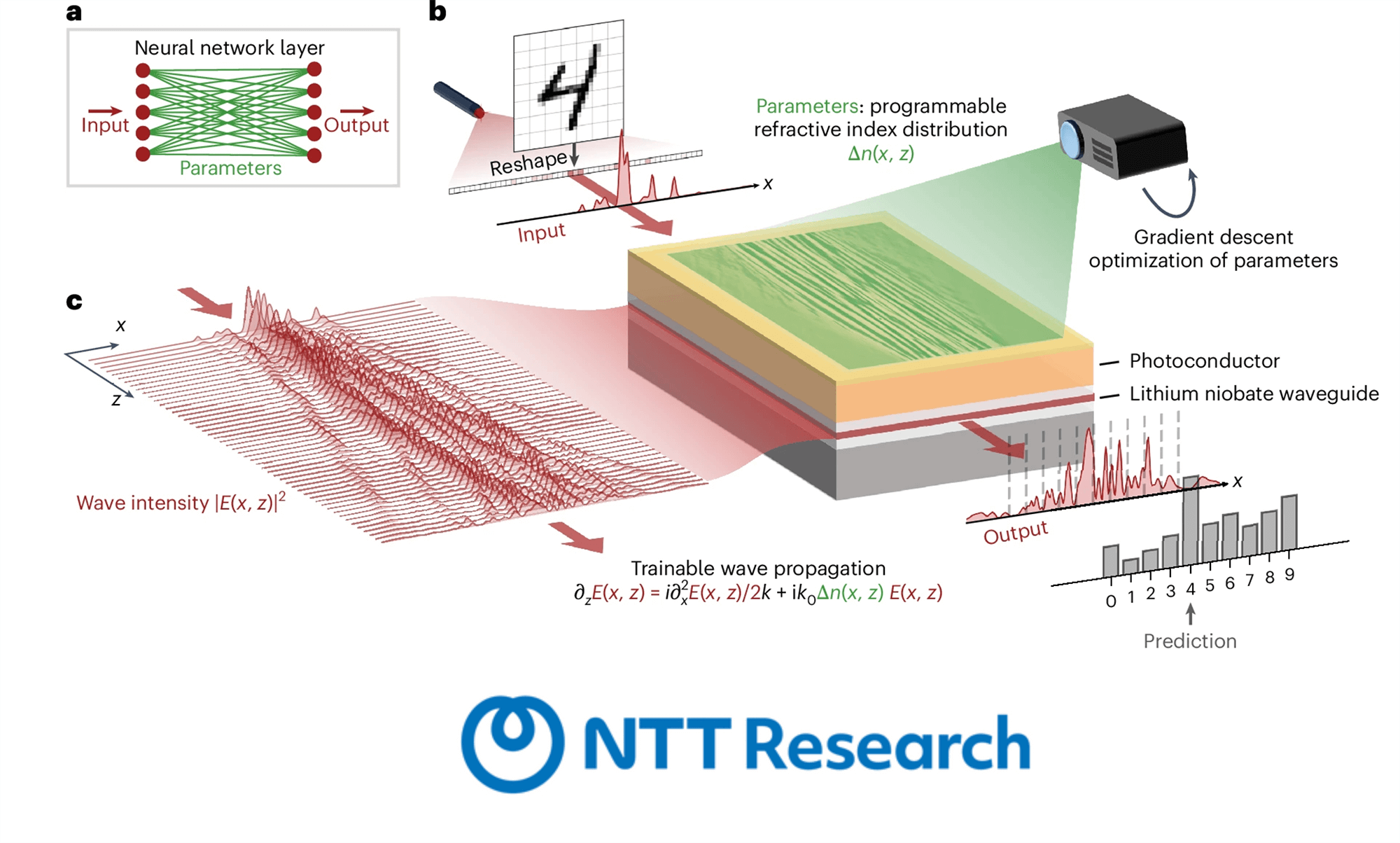
NTT Research unveiled a new lithium niobate–based programmable photonic waveguide that introduces a level of spatial control over light propagation not previously demonstrated in integrated optics. Developed with Cornell University and Stanford University, the two-dimensional slab waveguide provides roughly 10,000 programmable degrees of freedom, enabling the chip to execute machine-learning inference directly in the optical domain. The work appears in Nature Physics and extends earlier silicon-nitride research by the same team.
The device functions as an all-optical analogue to a neural-network layer, transforming input fields into output classifications in a single optical pass. Benchmark tests using up to 49-dimensional vectors yielded 96% vowel-classification accuracy and 86% performance on handwritten-digit recognition without any trainable electronic pre- or post-processing. The simplified fabrication process—beginning from a blank waveguide and then “painting” optical circuitry using illumination patterns—could reduce design overhead, mitigate manufacturing variability, and consolidate multiple photonic functions onto a single die.
This approach also points to new scaling behaviors. The authors report that two-dimensional programmable waveguides may reduce area growth from N² to approximately N^1.5 while increasing functional density. Although the device does not yet reach the mode count needed for clear energy-efficiency advantages over electronic accelerators, the researchers argue that the concept lays a foundation for higher-dimensional optical computing, advanced photonic routing, and free-space-style optical functionality on chip.
• Programmable lithium niobate waveguide with ~10,000 spatial degrees of freedom
• Fabricated as a uniform slab and programmed via projected light patterns acting as virtual electrodes
• Benchmarks: 96% accuracy (vowels), 86% accuracy (MNIST), single-pass optical inference
• Collaborators: NTT Research PHI Lab, Cornell University, Stanford University
• Potential applications: optical computing, datacenter signal routing, camera pre-processing, photonic simulation
• Scaling advantage: area through N^1.5 instead of N²; supports high spatial complexity
• Challenges ahead: increasing number of controllable modes for energy-efficient optical ML
“The device is a first of its kind, allowing us to essentially paint any optical circuitry we want and then redraw it in the blink of a second,” said Martin Stein, research scientist at NTT Research.
🌐 Analysis
This work reflects a growing push in programmable photonics toward architectures that avoid the overhead of thousands of discrete phase shifters, couplers, and electrodes. By shifting programmability into the optical field itself, NTT Research, Cornell, and Stanford align with broader industry efforts to improve reconfigurability and yield—areas that silicon photonics startups and labs have increasingly targeted. The lithium niobate platform, already gaining traction for modulators and nonlinear optics, now shows potential for adaptive on-chip computing architectures, complementing recent advances from both academic and commercial photonics groups.
🌐 We’re tracking the latest developments in semiconductors. Follow our ongoing coverage at: https://convergedigest.com/category/semiconductors/
🌐 We’re launching the “Data Center Networking for AI” series on NextGenInfra.io and inviting companies building real solutions—silicon, optics, fabrics, switches, software, orchestration—to share their views on video and in our expert report. To get involved, send a note to [email protected] or [email protected].