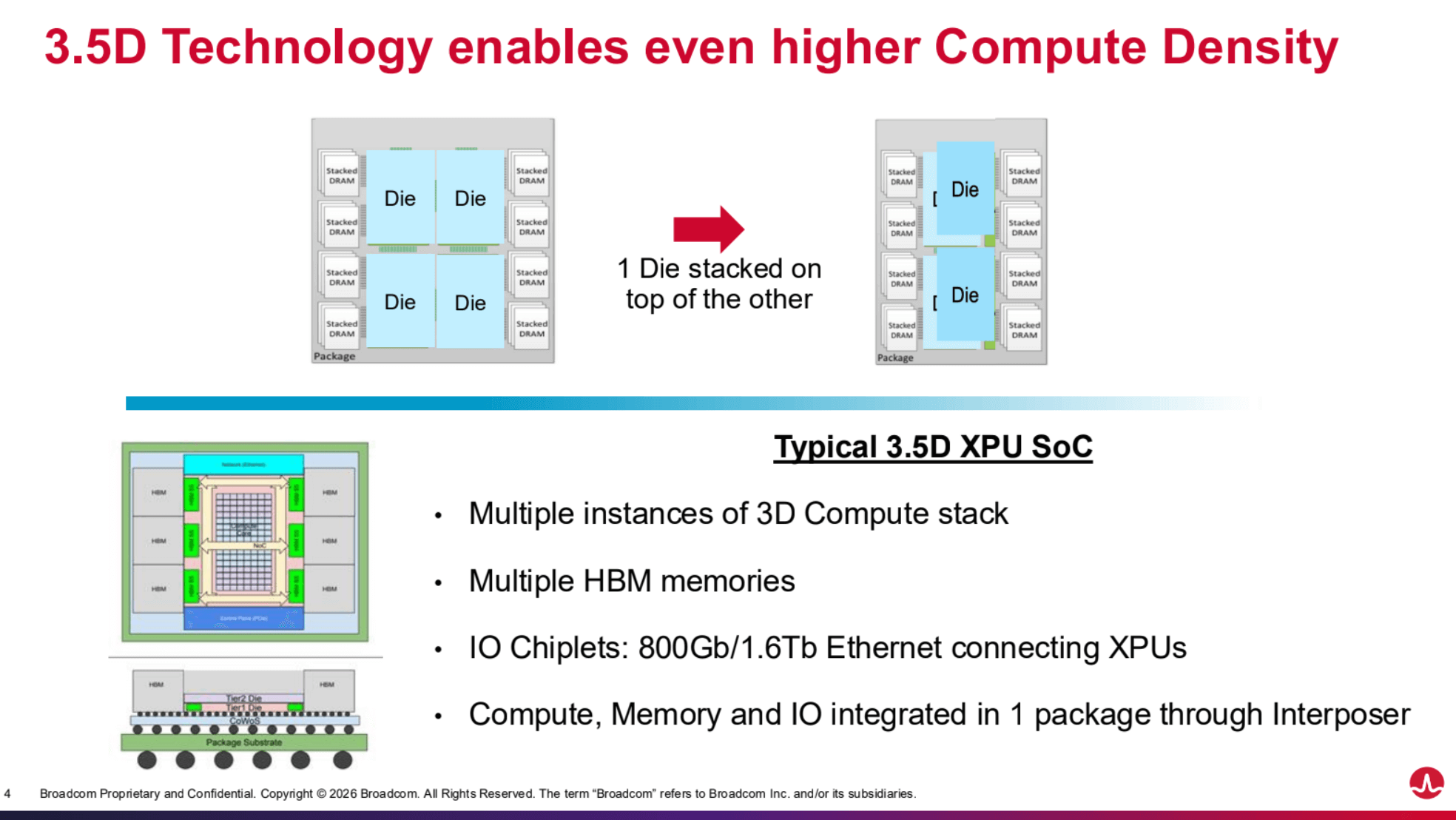
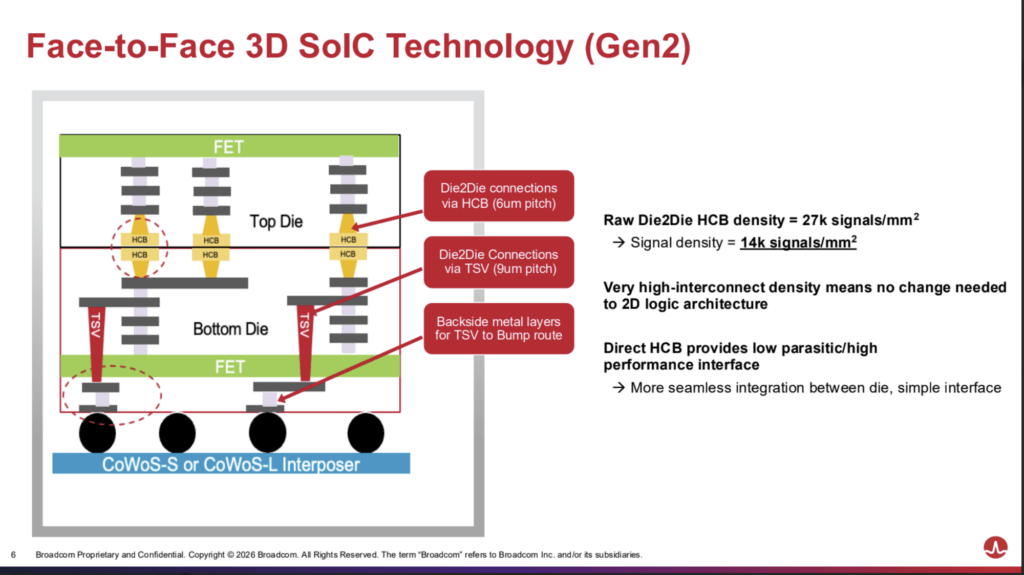
Broadcom Inc. has begun shipping what it describes as the industry’s first 2nm custom compute SoC built on its 3.5D eXtreme Dimension System in Package (XDSiP) platform. The device uses 3.5D Face-to-Face (F2F) die stacking technology to enable large-scale integration of XPUs designed for AI and high-performance computing workloads. Broadcom said the modular, multi-dimensional stacked die architecture combines 2.5D interposer techniques with 3D-IC integration to deliver higher signal density, improved power efficiency, and reduced latency within AI cluster deployments.
The 3.5D XDSiP platform allows compute, memory, and network I/O resources to scale independently within a compact form factor. Broadcom positions the technology as foundational for next-generation XPUs supporting gigawatt-scale AI clusters, where packaging density, power consumption, and die-to-die bandwidth have become limiting factors. By leveraging 2nm process technology alongside F2F 3D stacking, the platform increases compute density while optimizing energy efficiency. Broadcom previously introduced the 3.5D XDSiP platform in 2024 and said additional XPU programs based on the architecture are scheduled to ship in the second half of 2026.
The first 2nm 3.5D compute SoC ships to Fujitsu Limited and supports the company’s FUJITSU-MONAKA processor initiative. According to Fujitsu, the combination of advanced-node silicon and Face-to-Face 3D integration enables higher compute density and energy efficiency required for AI and HPC systems. Broadcom’s ASIC Products Division led development of the device as part of its custom XPU portfolio targeting hyperscale and enterprise AI deployments.
• First 2nm custom compute SoC built on 3.5D XDSiP platform
• Combines 2.5D interposer integration with 3D Face-to-Face die stacking
• Enables independent scaling of compute, memory, and network I/O
• Targets XPUs for gigawatt-scale AI cluster deployments
• Additional 3.5D-based XPU programs expected to ship in 2H 2026
“We’re proud to deliver the first 3.5D custom compute SoC for Fujitsu – a testament to the outstanding execution and innovation by the Broadcom team,” said Frank Ostojic, senior vice president and general manager of Broadcom’s ASIC Products Division.
🌐 Analysis: Broadcom’s shipment of a 2nm 3.5D compute SoC marks a transition from platform announcement to production silicon, reinforcing its position in custom AI accelerator engagements with large system vendors. The integration of advanced-node logic with Face-to-Face stacking reflects a broader industry shift toward hybrid bonding and vertical integration as scaling constraints tighten.
For Fujitsu, the collaboration supports its FUJITSU-MONAKA processor roadmap and signals continued investment by system OEMs in differentiated AI compute architectures rather than reliance solely on merchant GPUs. As additional 3.5D XDSiP programs move toward 2H 2026 production, competition in advanced packaging and custom XPU design is likely to intensify across hyperscale AI infrastructure.
🌐 We’re tracking the latest developments in networking silicon. Follow our ongoing coverage at: https://convergedigest.com/category/semiconductors/