NLM Photonics introduced new validation results and silicon-organic hybrid (SOH) photonic integrated circuit (PIC) samples at OFC 2026, highlighting progress with GlobalFoundries and Tower Semiconductor. The company demonstrated compatibility of its Selerion™-HTX organic electro-optic material with Tower’s PH18M silicon photonics platform and announced sampling of 1.6T and 3.2T PICs fabricated on GlobalFoundries’ advanced AMF processes. The work aims to extend the performance and efficiency of silicon photonics for AI data center interconnects without requiring major changes to existing foundry infrastructure.
At the core of NLM’s approach is its silicon-organic hybrid modulator technology, which integrates high-performance organic electro-optic materials into standard silicon photonics flows. According to the company, the SOH approach enables operation beyond 100 GHz bandwidth and supports 200G and 400G per-lane data rates while reducing device size by approximately 40% compared to conventional silicon photonics implementations. Initial results from Tower’s MPW run confirm process compatibility, while ongoing Process Development Kit (PDK) work is expected to formalize integration for broader ecosystem adoption.
In parallel, NLM taped out second-generation PICs in collaboration with Epiphany Design on GlobalFoundries’ AMF HP process, signaling a path toward scalable manufacturing. CEO Brad Booth emphasized that the company’s strategy centers on delivering a manufacturable “process blueprint” rather than discrete components—enabling foundries and system vendors to incorporate SOH materials into existing supply chains. He noted that this approach addresses key industry constraints around power consumption, device scaling, and integration across pluggable and co-packaged optics architectures.
- Validated SOH modulators on Tower Semiconductor’s PH18M silicon photonics platform via MPW run
- Sampled 1.6T and 3.2T PICs on GlobalFoundries AMF GP and HP processes
- Demonstrated >110 GHz bandwidth performance targeting 200G and 400G per-lane operation
- Achieved ~40% reduction in PIC footprint versus traditional silicon photonics
- Enabled integration using standard silicon photonics manufacturing flows (no dedicated fab line required)
- Advancing PDK development for both Tower and GlobalFoundries ecosystems
- Positioned SOH as a “fab-friendly” path to higher bandwidth and lower power optical interconnects
“Silicon photonic foundries are looking for a path to higher bandwidths, and SOH is a technology gaining interest as a ‘fab-friendly’ approach,” said Brad Booth, CEO of NLM Photonics. “The modulators are showing good initial performance, and as we refine the processing to achieve optimal results, we see a clear roadmap to 400G per lane.”
🌐 Interview
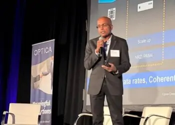
Q&A: Jim Carroll Interviews Brad Booth, CEO of NLM Photonics
Jim Carroll: We’re seeing massive growth in AI data centers. From your perspective, what is the core challenge the industry is trying to solve?
Brad Booth: The fundamental issue is that the incumbent technologies we’ve relied on—especially silicon photonics—are starting to hit limits as we move to higher data rates. At 200G per lane, you can still make it work, but power starts creeping up. At 400G per lane, power becomes a major constraint.
At the same time, some alternative technologies reduce power, but they don’t integrate well into future architectures like co-packaged optics. That creates a bifurcation—one set of technologies for pluggables and another for co-packaged optics. The industry doesn’t want that. It wants a unified platform that can scale across use cases.
Jim Carroll: So where does NLM fit into that challenge?
Brad Booth: We bring a material science approach that enhances existing silicon photonics platforms rather than replacing them. For example, by integrating our organic electro-optic material into a silicon photonics PIC, we can significantly reduce drive voltage and shrink device size.
In practical terms, a 1.6T PIC using our approach can be about 40% smaller than a traditional silicon photonics implementation, while still being manufactured in a standard silicon photonics process. That means better performance, lower power, and lower cost—all within the existing ecosystem.
Jim Carroll: There’s a lot of discussion about NLM as a materials company. What differentiates your approach?
Brad Booth: We are fundamentally a materials science company, but what’s unique is how we apply that. We’re not trying to sell a discrete product—we’re delivering a process.
We develop the materials, the device designs, and the integration steps, and then transfer that intellectual property to foundries and customers. Once they’re up and running, they can use it within their own manufacturing flows. That allows us to stay focused on advancing the next generation rather than supporting a single product line.
Jim Carroll: Can you talk about your materials portfolio and how it maps to different applications?
Brad Booth: We currently have multiple materials tailored to different use cases. Our Selerion™-HTX material is designed for data communications—it’s highly efficient and optimized for high-performance modulators.
We also have materials for very small devices, such as plasmonic structures, where size is critical, as well as materials aimed at quantum applications. The idea is to match the material properties to the device requirements, whether that’s bandwidth, size, or efficiency.
Jim Carroll: You’ve worked extensively with hyperscalers. How does that experience shape your strategy?
Brad Booth: Hyperscalers are extremely focused on supply chain scalability. It’s not enough to have a good technology—you need to scale from tens of units to millions or even hundreds of millions.
If we tried to build and sell components ourselves, it would require massive capital investment. Instead, we work with existing foundries and suppliers already in the ecosystem. We enhance their platforms with our materials and processes. That keeps our burn rate low and aligns with how hyperscalers actually want to procure technology.
Jim Carroll: How does your approach compare with other material platforms like lithium niobate?
Brad Booth: Lithium niobate delivers strong performance, but it typically requires dedicated fab lines because of contamination concerns. That creates barriers for integration into standard silicon photonics foundries.
Our materials are different—they behave more like a specialized photoresist and can be integrated into existing processes without contaminating the fab. That makes it much easier for foundries to adopt and scale.
Jim Carroll: Let’s talk about your OFC announcements. What progress have you made with GlobalFoundries and Tower Semiconductor?
Brad Booth: With GlobalFoundries, we’ve been working for a couple of years and used their platform to develop our 1.6T and 3.2T PICs. That gave us valuable insight into manufacturing challenges and validated that we can produce full PICs, not just individual modulators.
We’ve now completed additional tape-outs in their high-performance flow, and we’re already looking ahead to the next generation, including designs targeting 800G per lane.
With Tower Semiconductor, we demonstrated that their PH18 platform can support our silicon-organic hybrid modulators. We integrated our material into slot waveguides and are seeing encouraging results, including improved performance compared to standard implementations.
Jim Carroll: What feedback are you getting from the industry?
Brad Booth: The conversation has shifted. It’s no longer “this is interesting”—it’s “how do we bring this into our platform?”
Foundries and system companies are actively evaluating which technology paths to invest in. With the scale of AI infrastructure—millions of transceivers and massive switching deployments—there’s real urgency to identify solutions that can deliver both performance and manufacturability.
Jim Carroll: Final question—what does success look like for NLM over the next few years?
Brad Booth: Success is seeing our process adopted broadly across the ecosystem—foundries, design houses, and system vendors.
If we can enable higher performance while reducing power and cost, and do it within existing manufacturing infrastructure, then we’re helping the industry continue scaling. That’s the goal.
🌐 Analysis
NLM Photonics positions silicon-organic hybrid technology as an incremental—but potentially disruptive—extension of silicon photonics rather than a replacement. This aligns with hyperscaler supply chain priorities, where compatibility with existing foundries such as GlobalFoundries and Tower Semiconductor reduces adoption friction compared to alternatives like lithium niobate or plasmonics that often require specialized manufacturing. The company’s “process-first” model also reflects a broader industry trend toward platform enablement rather than discrete component competition.
The timing is notable as the industry pushes toward 200G and 400G per-lane signaling for 1.6T and 3.2T optics, where conventional silicon photonics faces increasing power and scaling challenges. Competing approaches—including thin-film lithium niobate, indium phosphide, and emerging electro-optic polymers—are all vying for position in next-generation AI interconnects. NLM’s ability to integrate organic materials into standard CMOS-compatible flows could provide a differentiated path if it achieves consistent manufacturability and long-term reliability at scale.