• Home
  • Events Calendar
  • Blueprint Guidelines
  • Privacy Policy
  • Subscribe to Daily Newsletter
  • NextGenInfra.io
No Result
View All Result
Converge Digest
Monday, May 25, 2026
  • Home
  • Events Calendar
  • Blueprint Guidelines
  • Privacy Policy
  • Subscribe to Daily Newsletter
  • NextGenInfra.io
No Result
View All Result
Converge Digest
No Result
View All Result

Home » Amkor Deepens U.S. Packaging Investment 

Amkor Deepens U.S. Packaging Investment 

May 22, 2026
in Semiconductors
A A

Amkor Technology is expanding its U.S. advanced packaging footprint with the acquisition of an additional 67-acre parcel adjacent to its semiconductor packaging and test campus in Peoria, Arizona. The move increases the company’s total Arizona footprint to 171 acres and provides additional room for future manufacturing capacity as demand rises for advanced packaging across AI, high-performance computing, automotive, and communications markets.

The Peoria site, located within the city’s Innovation Core district, is already under development as a large-scale advanced semiconductor packaging and test facility. Amkor has said the campus is expected to become the first high-volume advanced packaging OSAT facility in the United States. The additional land gives the company strategic flexibility to scale operations over time as customers increase demand for more sophisticated packaging technologies such as chiplets, 2.5D and 3D integration, system-in-package, and advanced test.

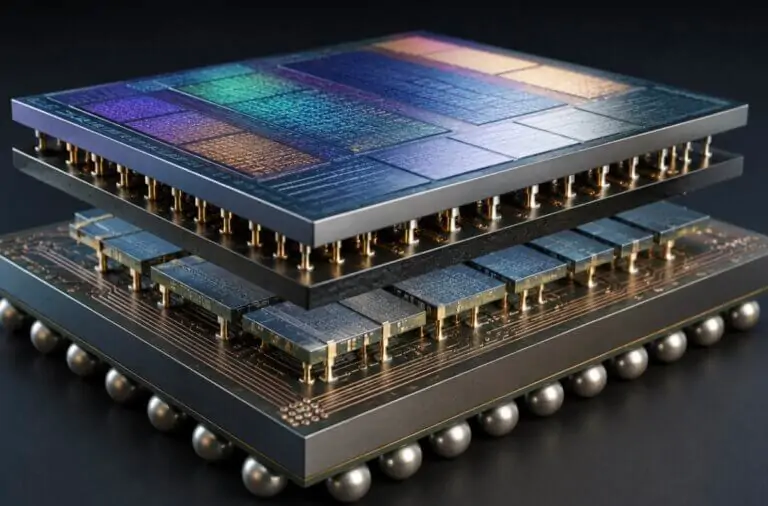
The expansion comes amid growing focus on semiconductor packaging as a critical layer of AI infrastructure. While much attention in recent years has centered on U.S.-based wafer fabrication, advanced packaging has become increasingly important for integrating GPUs, accelerators, high-bandwidth memory, and heterogeneous compute platforms. Amkor’s investment strengthens domestic packaging capacity at a time when the U.S. semiconductor industry is working to build a more resilient supply chain across both front-end manufacturing and backend assembly.

Profile: Amkor Arizona Expansion

CategoryDetails
New Land Acquisition67 acres adjacent to existing Peoria campus
Existing Campus Size104 acres
Total Arizona Footprint171 acres (approximately 69 hectares)
Facility FocusAdvanced semiconductor packaging and test
Target ApplicationsArtificial intelligence, HPC, automotive, communications
Core TechnologiesAdvanced packaging, wafer-level processing, system-in-package, semiconductor test
Strategic ImportanceExpected to be the first high-volume advanced packaging OSAT facility in the United States

“Amkor’s investment in Arizona represents a significant step in building advanced semiconductor manufacturing capacity in the United States,” said Kevin Engel, president and chief executive officer of Amkor Technology. “Our continued expansion in Arizona strengthens our ability to support customers with leading-edge packaging and test solutions while contributing to a more resilient global supply chain.”

🌐 Analysis: Amkor’s Arizona expansion highlights how advanced packaging is becoming a strategic battleground in the semiconductor industry. AI accelerators increasingly rely on advanced packaging techniques to integrate logic dies with high-bandwidth memory and dense interconnects, making backend manufacturing a critical part of overall system performance. The Peoria site places Amkor closer to a growing cluster of U.S.-based semiconductor manufacturing activity, including investments by TSMC, Intel, and Micron Technology.

🌐 We’re tracking the latest developments in networking silicon. Follow our ongoing coverage at: https://convergedigest.com/category/semiconductors/

Tags: Amkor
ShareTweetShareSummarizeSummarize
Previous Post

UCLA Launches $125M Semiconductor Hub

Jim Carroll

Jim Carroll

Editor and Publisher, Converge! Network Digest, Optical Networks Daily - Covering the full stack of network convergence from Silicon Valley

Related Posts

Semiconductors

Amkor Expands AZ Investment to $7B for Advanced Semiconductor Packaging Campus

October 6, 2025

Categories

  • 5G / 6G / Wi-Fi
  • AI Infrastructure
  • All
  • Automotive Networking
  • Blueprints
  • Clouds and Carriers
  • Data Centers
  • Enterprise
  • Explainer
  • Feature
  • Financials
  • Last Mile / Middle Mile
  • Legal / Regulatory
  • Optical
  • Quantum
  • Research
  • Security
  • Semiconductors
  • Space
  • Start-ups
  • Subsea
  • Sustainability
  • Video
  • Webinars

Archives

Tags

5G All AT&T Australia AWS Blueprint columns BroadbandWireless Broadcom China Ciena Cisco Data Centers Dell'Oro Ericsson FCC Financial Financials Huawei Infinera Intel Japan Juniper Last Mile Last Mille LTE Mergers and Acquisitions Mobile NFV Nokia Optical Packet Systems PacketVoice People Regulatory Satellite SDN Service Providers Silicon Silicon Valley StandardsWatch Storage TTP UK Verizon Wi-Fi
Converge Digest

A private dossier for networking and telecoms

Follow Us

  • Home
  • Events Calendar
  • Blueprint Guidelines
  • Privacy Policy
  • Subscribe to Daily Newsletter
  • NextGenInfra.io

© 2026 Converge Digest - A private dossier for networking and telecoms.

No Result
View All Result
  • Home
  • Events Calendar
  • Blueprint Guidelines
  • Privacy Policy
  • Subscribe to Daily Newsletter
  • NextGenInfra.io

© 2026 Converge Digest - A private dossier for networking and telecoms.

This website uses cookies. By continuing to use this website you are giving consent to cookies being used. Visit our Privacy and Cookie Policy.
Go to mobile version