Applied Materials introduces new deposition systems targeting angstrom-era logic nodes, as chipmakers transition to Gate-All-Around (GAA) transistor architectures at 2nm and beyond. The company unveiled its Precision™ Selective Nitride PECVD and Endura™ Trillium™ ALD systems on April 8, positioning both as enabling technologies for atomic-scale materials engineering required in next-generation AI processors.
The announcement reflects growing process complexity in advanced logic manufacturing, where GAA transistors require more than 500 process steps and extremely tight tolerances approaching atomic dimensions. Applied Materials said its new systems focus on improving deposition precision for both insulating dielectrics and metal gate stacks—two critical elements that directly impact transistor performance, power efficiency, and yield. The company noted that both systems are already being adopted by leading foundry and logic customers at 2nm-class nodes.
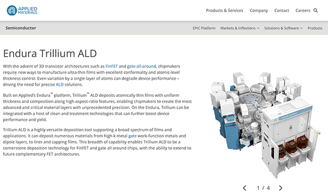
The Precision Selective Nitride PECVD system targets shallow trench isolation (STI), a key structure used to electrically isolate transistors. The system applies a selective bottom-up deposition of silicon nitride to reinforce silicon oxide trenches, helping preserve their integrity through subsequent processing steps. This approach reduces parasitic capacitance and leakage, improving performance-per-watt. Meanwhile, the Trillium ALD system focuses on metal gate stack formation in GAA transistors, where nanosheets spaced roughly 10 nanometers apart must be fully wrapped with uniform metal layers. By integrating multiple deposition steps within a high-vacuum environment, the system enables angstrom-level control of metal thickness and supports tuning of transistor characteristics for different AI workloads.
- Applied Materials introduced Precision Selective Nitride PECVD and Trillium ALD systems on April 8, 2026
- Systems are designed for 2nm and beyond Gate-All-Around (GAA) transistor nodes
- Precision PECVD reinforces shallow trench isolation to reduce parasitic capacitance and leakage
- Trillium ALD enables uniform metal gate stack deposition across nanosheet structures spaced ~10 nm apart
- Both systems support atomic-scale deposition control to improve performance, power efficiency, and yield
- Technologies are already being adopted by leading foundry-logic manufacturers
- GAA transistor fabrication can require 500+ process steps with atomic-level tolerances
“Our industry is entering a period of rapid, non-linear change, where traditional lithographic chip scaling alone is no longer sufficient,” said Dr. Prabu Raja, President of the Semiconductor Products Group at Applied Materials. “At the most advanced angstrom-class logic nodes, performance and power are increasingly determined by materials.”
🌐 Analysis: Applied Materials continues to position materials engineering as the primary lever for scaling beyond traditional lithography, particularly as the industry transitions from FinFET to GAA architectures at 2nm and below. The emphasis on deposition precision aligns with broader industry trends, where variability, power efficiency, and yield challenges are increasingly tied to atomic-scale materials control rather than geometric scaling alone. Competing equipment vendors, including Lam Research and Tokyo Electron, are also focusing on advanced deposition and etch innovations, but Applied’s integration of multi-step processes and vacuum environments highlights a systems-level approach to solving GAA complexity.
🌐 We’re tracking the latest developments in networking silicon. Follow our ongoing coverage at: https://convergedigest.com/category/semiconductors/
🌐 We’re launching the “Data Center Networking for AI” series on NextGenInfra.io and inviting companies building real solutions—silicon, optics, fabrics, switches, software, orchestration—to share their views on video and in our expert report. To get involved, send a note to [email protected] or [email protected].