Atomera announced new test results showing that its Mears Silicon Technology (MST) can address a longstanding challenge that has limited the adoption of gallium nitride (GaN) devices on silicon substrates for high-frequency RF applications. The company said its approach reduces parasitic channel losses that have historically degraded the performance of GaN-on-Silicon devices, particularly at higher frequencies. By improving RF efficiency and linearity, Atomera aims to make lower-cost silicon substrates a viable alternative to silicon carbide (SiC) for applications such as 5G, future 6G systems, and other high-frequency wireless infrastructure.
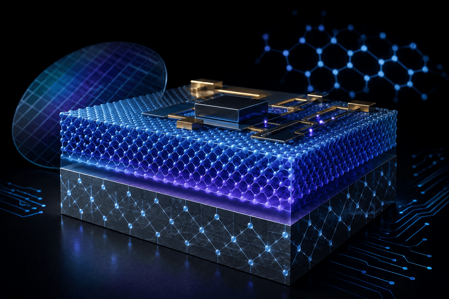
Today, most high-performance RF GaN devices rely on SiC substrates because of their superior electrical characteristics, despite higher manufacturing costs and limited wafer scalability. Atomera’s MST process inserts a thin oxygen-modified layer near the silicon surface, improving the GaN/silicon interface by modifying lattice characteristics and reducing dopant diffusion. According to the company, testing demonstrated more than a 10x reduction in parasitic channel charge, helping reduce RF power losses while supporting improved high-frequency performance.
Independent RF characterization by Incize found substantial improvements in both small-signal and large-signal performance. Atomera reported that MST-enabled GaN-on-Silicon samples delivered significantly improved linearity and power handling, with linearity measurements at a 30 mW benchmark input power reportedly reaching levels approximately 1,000 times better than a reference GaN-on-Silicon wafer. The company also stated that the performance benefits extended up to 10W input power, approaching characteristics typically associated with advanced RF SOI technologies.
- MST introduces an oxygen-modified layer within the silicon substrate to improve GaN growth.
- Testing showed more than a 10x reduction in parasitic channel charge.
- Improved RF linearity and reduced RF losses were demonstrated in GaN-on-Silicon devices.
- Performance improvements were observed from low-power operation through 10W input power levels.
- The technology could reduce dependence on more expensive silicon carbide substrates.
- Target applications include 5G, future 6G, RF front-end modules, wireless infrastructure, aerospace, defense, and power electronics.
“Atomera’s MST is removing barriers to GaN-on-Silicon-based RF systems, unlocking breakthrough RF performance on low-cost silicon substrates,” said Scott Bibaud, president and CEO of Atomera.
🌐 Analysis: GaN-on-Silicon has long attracted industry interest because it offers the manufacturing scale, larger wafer sizes, and lower costs of conventional silicon fabs. However, RF performance limitations have prevented widespread displacement of GaN-on-SiC in demanding wireless infrastructure applications. Atomera’s latest results focus directly on one of the key technical barriers—parasitic interface effects that degrade efficiency and linearity at higher frequencies.
🌐 The announcement also aligns with broader industry efforts to improve the economics of RF semiconductors as 5G networks mature and research into 6G architectures accelerates. Semiconductor suppliers including GlobalFoundries, TSMC, Tower Semiconductor, and Wolfspeed continue to invest in RF technologies spanning RF SOI, GaN, and SiC platforms. If Atomera can validate these gains in commercial manufacturing environments, MST could expand the addressable market for GaN-on-Silicon across both RF and power device segments.
| Category | Details |
|---|---|
| Company | Atomera Incorporated (NASDAQ: ATOM) |
| Headquarters | Los Gatos, California, USA |
| Founded | 2001 |
| Leadership | Scott Bibaud (President & CEO); Dr. Robert Mears (Founder & CTO) |
| Core Technology | Mears Silicon Technology (MST): A quantum-engineered, thin-film atomic layer of oxygen inserted into silicon to control dopant diffusion, reduce leakage, and improve mobility. |
| Business Model | Semiconductor materials IP licensing, technology transfer, and collaborative development. |
| Technology Focus | Performance, linearity, and power efficiency enhancement for CMOS, advanced nodes (GAA), RF, power devices (GaN/SiC), and silicon photonics. |
| Key Advantage | Seamless integration into existing commercial semiconductor fabrication lines using standard epitaxy equipment with minimal process flow changes. |
| Recent Milestones (2026) |
|
| Target Markets | 5G/6G RF infrastructure, power electronics (EVs, smart grid), AI infrastructure, mobile/RF SOI alternatives, and advanced foundry logic. |

