• Home
  • Events Calendar
  • Blueprint Guidelines
  • Privacy Policy
  • Subscribe to Daily Newsletter
No Result
View All Result
Converge Digest
  • Home
  • Events Calendar
  • Blueprint Guidelines
  • Privacy Policy
  • Subscribe to Daily Newsletter
No Result
View All Result
Converge Digest
No Result
View All Result

Home » Avicena shows its microLED-based LightBundle multi-Tbps interconnect

Avicena shows its microLED-based LightBundle multi-Tbps interconnect

November 15, 2023
in Optical
A A

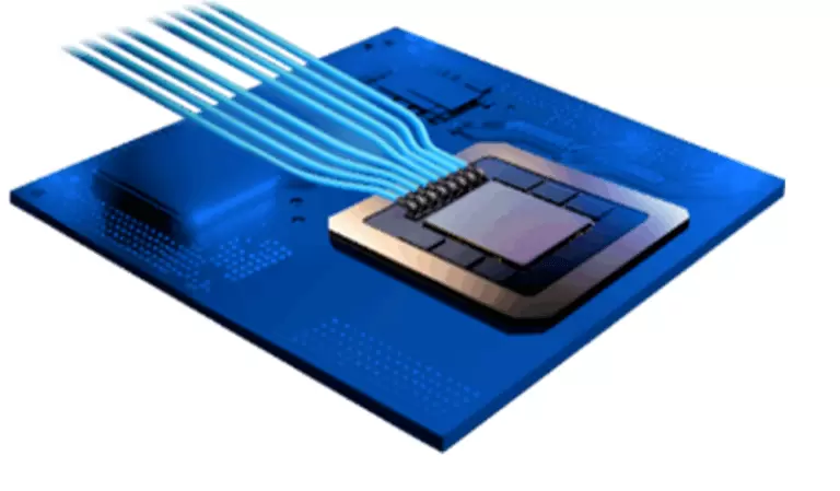
At this week’s SuperComputing Conference (SC23) in Denver, Avicena is demonstrating its 1 Tbps optical transceiver as part its microLED-based LightBundle multi-Tbps chip-to-chip interconnect technology.

Currently, high-bandwidth memory (HBM) modules must be co-packaged with GPUs because the GPU-memory electrical interconnect is limited to just a few millimeters in length. Subsequent HBM generations will require IC shoreline densities in the range of 10 Tbps/mm or more.

Avicena says conventional optical interconnects based on VCSELs or Silicon Photonics (SiPh) promise to extend the interconnect reach but struggle to meet size, bandwidth density, power, latency, operating temperature, and cost requirements. Its microLED-based LightBundle interconnects provide higher bandwidth density, much smaller size, much lower power and latency, and very low costs.

“At Avicena we are excited to showcase the world’s most compact 1Tbps transceiver in the shape of a 3mm x 4mm CMOS ASIC using our patented microLED optical interface,” says Bardia Pezeshki, Founder and CEO of Avicena. “Everyone is talking about SiPh solutions for applications in AI clusters. However, for short reach interconnects with less than 10m reach, we believe that our LED based solution is inherently better suited because the compact size, higher bandwidth density, lower power and latency, and temperature tolerance up to 150°C.”

Tags: Avicena
ShareTweetSend
Previous Post

Canada to open FTTH in Ontario and Québec, Bell to cut capex

Next Post

Argonne’s trillion parameter Aurora genAI project leverages Intel GPUs

Related Posts

Avicena develops highly parallel optical interconnect for chips
All

Avicena develops highly parallel optical interconnect for chips

June 9, 2021
Next Post
Argonne’s trillion parameter Aurora genAI project leverages Intel GPUs

Argonne's trillion parameter Aurora genAI project leverages Intel GPUs

Download our New Middle Mile Report

Categories

  • 5G / 6G / Wi-Fi
  • All
  • Automotive Networking
  • Blueprints
  • Clouds and Carriers
  • Data Centers
  • Enterprise
  • Financials
  • Last Mile / Middle Mile
  • Optical
  • Quantum
  • Research
  • Security
  • Semiconductors
  • Space
  • Start-ups
  • Subsea
  • Sustainability
  • Video
  • Webinars

Archives

Tags

5G All AT&T AWS Blueprint columns BroadbandWireless Broadcom China Ciena Cisco Data Centers Dell'Oro Ericsson FCC Financial Financials Huawei Infinera Intel Japan Juniper Last Mile Last Mille LTE Mergers and Acquisitions Mobile NFV Nokia Optical Packet Systems PacketVoice People Regulatory Satellite SDN Security Service Providers Silicon Silicon Valley StandardsWatch Storage TTP UK Verizon Wi-Fi
Converge Digest

A private dossier for networking and telecoms

Follow Us

Recent News

Amazon’s Project Kuiper signs NTT/SKY Perfect JSAT

Amazon’s Project Kuiper signs NTT/SKY Perfect JSAT

November 28, 2023
Verizon demos 5G network slicing for Axon public safety

Verizon demos 5G network slicing for Axon public safety

November 28, 2023
  • Home
  • Events Calendar
  • Blueprint Guidelines
  • Privacy Policy
  • Subscribe to Daily Newsletter

© 2023 Converge Digest - A private dossier for networking and telecoms.

No Result
View All Result
  • Home
  • Events Calendar
  • Blueprint Guidelines
  • Privacy Policy
  • Subscribe to Daily Newsletter

© 2023 Converge Digest - A private dossier for networking and telecoms.

This website uses cookies. By continuing to use this website you are giving consent to cookies being used. Visit our Privacy and Cookie Policy.
Go to mobile version