Former Broadcom engineer charged with stealing secrets
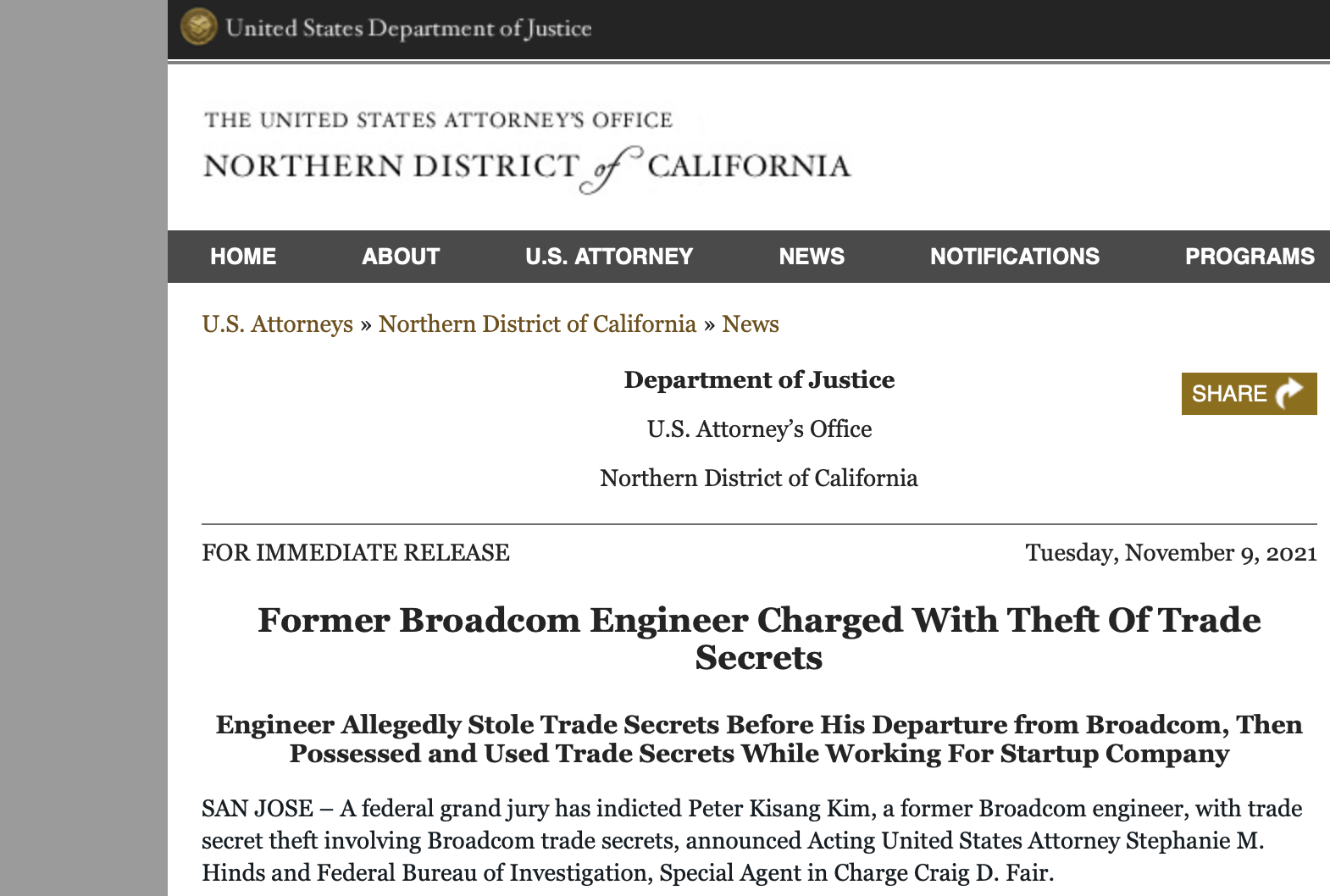
Peter Kisang Kim, a former Broadcom engineer, has been indicted by a U.S. federal grand jury on 18 charges of trade secret theft.The indictment alleges that Kim worked as a...
Silicon for AI, Cloud, Telecom and Digital Infrastructure Converge Digest tracks the semiconductor platforms powering next-generation networks, AI clusters, optical systems, data centers, wireless infrastructure and edge devices. |
Silicon Pillars AI AcceleratorsNetworking SiliconOptical DSPsChipletsMemorySilicon PhotonicsWireless SoCs |
| Tracking: Tapeouts • Process Nodes • Packaging • Foundry Partnerships • AI Inference • Ethernet Switching • Coherent Optics • Memory Bandwidth • Power Efficiency • Supply Chain |
Peter Kisang Kim, a former Broadcom engineer, has been indicted by a U.S. federal grand jury on 18 charges of trade secret theft.The indictment alleges that Kim worked as a...
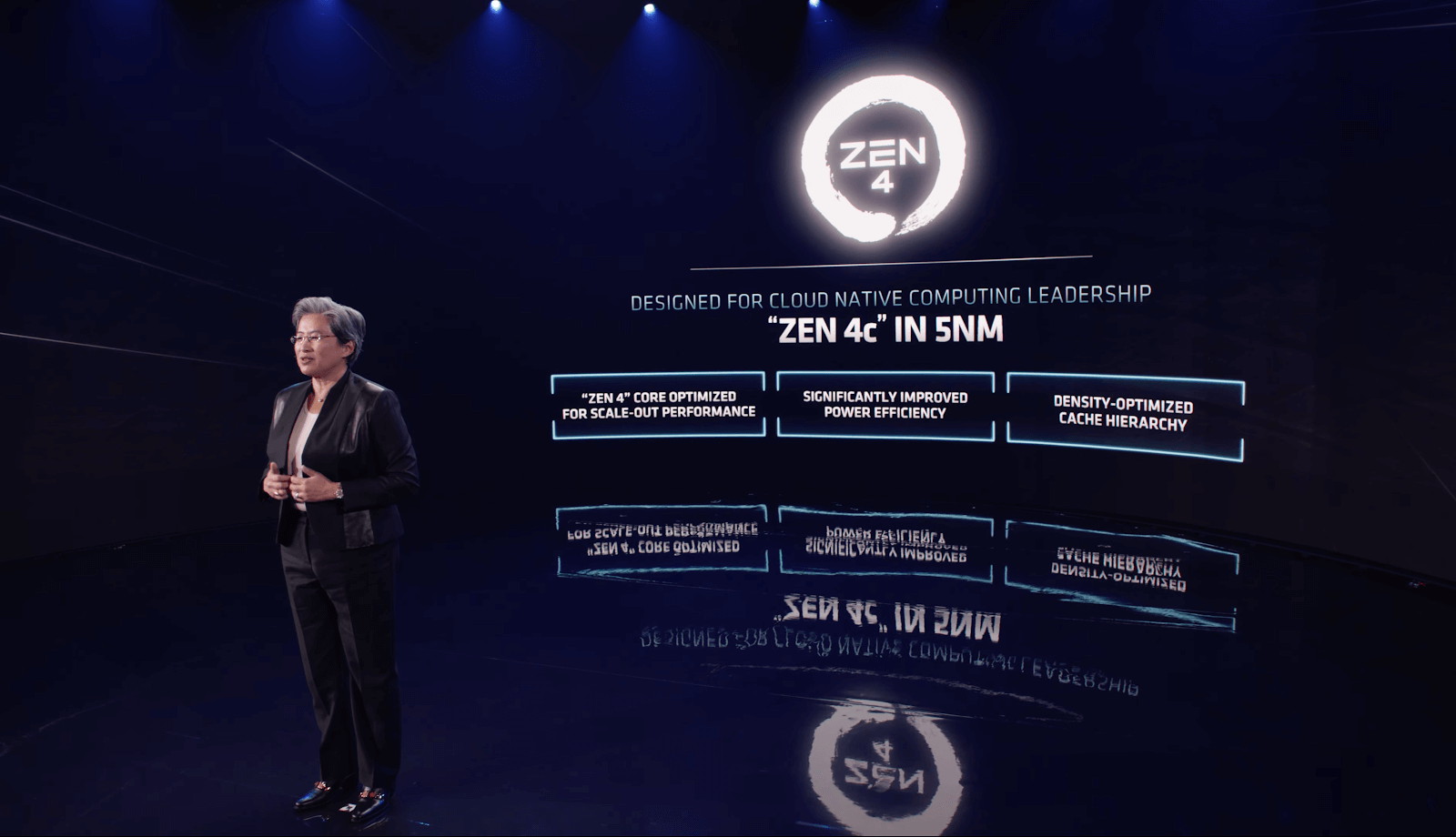
At a virtual event ahead of this week's Open Compute Project Summit, Dr. Lisa Su, president and CEO of AMD, introduced the company's Instinct MI200 series accelerators for high performance...

Intel launched the first products in the 12th Gen Intel Core family, boasting faster processing and the latest connectivity standards. The family includes six new unlocked desktop processors offering a...

Renesas Electronics agreed to acquire Celeno Communications, a start-up providing Wi-Fi solutions, for approximately US$315 million (approximately 35.9 billion yen at an exchange rate of 114 yen to the dollar)...

Cisco has begun sampling its latest P100 routing silicon, the 11th device in the Cisco Silicon One family which debuted in December 2019.The 7nm Cisco Silicon One P100 boasts the...

Hailo, a start-up based in Tel Aviv, raised $136 million in a Series C round of funding for its edge processor designed for AI workloads.The Hailo-8 edge AI processor boasts...

Samsung Foundry is scheduled to start producing its customers' first 3nm-based chip designs in the first half of 2022, while its second generation of 3nm is expected in 2023.During its...

Cadence Design Systems released its Integrity 3D-IC platform integrating 3D chip design planning, implementation and system analysis.Cadence says its platform provides system planning, integrated electrothermal, static timing analysis (STA) and...

Marvell will use TSMC’s 3nm process technology to offer custom silicon for cloud data center, 5G carrier, automotive and enterprise markets.Marvell is first to introduce a silicon platform that leverages...

Marvell announced the availability of its 5nm Prestera DX 7321 Ethernet switch, the industry’s first 5nm 50G PAM4 device for the carrier market.The new Marvell Prestera switch is designed for...
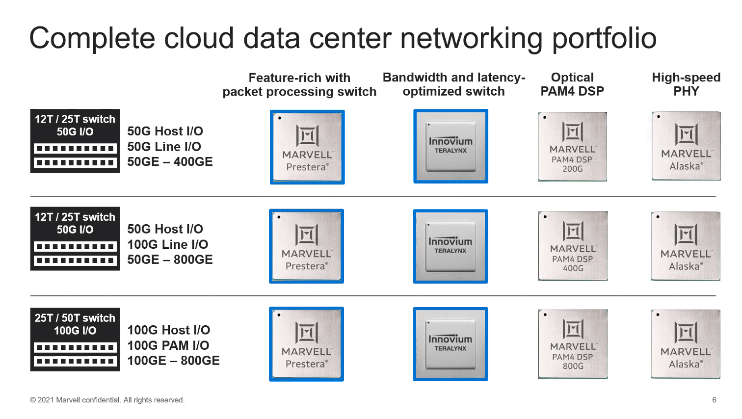
Marvell Technology completed its previously announced acquisition of Innovium. Marvell to acquire Innovium for data center switching siliconTuesday, August 03, 2021 Innovium, Marvel Marvell Technology agreed to acquire Innovium, a start-up offering switching silicon...

Astera Labs, a start-up based in Santa Clara, California, raised $50 million in an over subscribed Series-C funding round for its silicon solutions for intelligent systems.Astera Labs recently launched its...
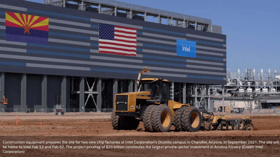
Intel broke ground on two new fabs (52 and 62) at the company’s Ocotillo campus in Chandler, Arizona. When fully operational in 2024, the new fabs will manufacture Intel’s most...


A private dossier for networking and telecoms