
• Home
  • About
  • Events Calendar
  • Blueprint Guidelines
  • Privacy Policy
  • Manage Email Delivery
  • NextGenInfra.io
  • buzzwords
  • Archives
  • Milestones
  • On This Day
  • Video Search
Converge Digest
Wednesday, July 15, 2026
  • Home
  • About
  • Events Calendar
  • Blueprint Guidelines
  • Privacy Policy
  • Manage Email Delivery
  • NextGenInfra.io
  • buzzwords
  • Archives
  • Milestones
  • On This Day
  • Video Search
No Result
View All Result
Converge Digest
No Result
View All Result

Home » IBM Kicks off $3 Billion Silicon Research Initiative

IBM Kicks off $3 Billion Silicon Research Initiative

July 9, 2014
in All, Silicon Photonics
A A

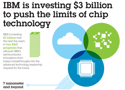
IBM announced a $3 billion research initiative that aims to advance silicon technologies to the 7nm threshold or below.  Over the next 5 years, IBM will conduct two broad research and early stage development programs.

The first is aimed at so-called “7 nanometer and beyond” silicon technology and the second is focused on developing alternative technologies for post-silicon era chips using entirely different approaches.

IBM said its research teams will be able to leverage work it already has underway in area such as carbon nanoelectronics, silicon photonics, new memory technologies, and architectures that support quantum and cognitive computing.

“The question is not if we will introduce 7 nanometer technology into manufacturing, but rather how, when, and at what cost?” said John Kelly, senior vice president, IBM Research. “IBM engineers and scientists, along with our partners, are well suited for this challenge and are already working on the materials science and device engineering required to meet the demands of the emerging system requirements for cloud, big data, and cognitive systems. This new investment will ensure that we produce the necessary innovations to meet these challenges.”

https://www-03.ibm.com/press/us/en/pressrelease/44357.wss

Tags: Blueprint columnsIBMSilicon
ShareTweetShareSummarizeSummarize
Previous Post

Colombia’s UNE EPM Deploys 100G with ALU

Next Post

Qualcomm Supports Docomo’s VoLTE Launch in Japan

Staff

Staff

Related Posts

All

IBM Brings z17 to Standard Data Center Racks

July 7, 2026
Semiconductors

IBM Reveals 0.7 nm Chip with 3D Nanostack Architecture

June 25, 2026
All

IBM, Red Hat and Palo Alto Networks Launch Project Lightwell

June 24, 2026
Quantum

IBM Commits $10 Billion to Quantum Computing

June 3, 2026
Quantum

IBM and U.S. Commerce Plan $2B Quantum Foundry Company in Albany

May 21, 2026
Enterprise

IBM and Arm Signal Shift Toward Heterogeneous Enterprise Compute

April 6, 2026
Next Post

Qualcomm Supports Docomo's VoLTE Launch in Japan

Please login to join discussion

Categories

  • 5G / 6G / Wi-Fi
  • AI Infrastructure
  • All
  • Automotive Networking
  • Blueprints
  • Clouds and Carriers
  • Corporate Strategies
  • CPO
  • Data Centers
  • Enterprise
  • Explainer
  • Feature
  • Hot Start-ups
  • Last Mile / Middle Mile
  • Legal / Regulatory
  • Optical
  • Optical I/O
  • Pluggable Optics
  • Quantum
  • Research
  • Security
  • Semiconductors
  • Silicon Photonics
  • Space Networking & Orbital Data Centers
  • Subsea
  • Sustainability
  • Video
  • Webinars
Converge Digest

A private dossier for networking and telecoms

Follow Us

  • Home
  • About
  • Events Calendar
  • Blueprint Guidelines
  • Privacy Policy
  • Manage Email Delivery
  • NextGenInfra.io
  • buzzwords
  • Archives
  • Milestones
  • On This Day
  • Video Search

© 2026 Converge Digest - A private dossier for networking and telecoms.

No Result
View All Result
  • Home
  • About
  • Events Calendar
  • Blueprint Guidelines
  • Privacy Policy
  • Manage Email Delivery
  • NextGenInfra.io
  • buzzwords
  • Archives
  • Milestones
  • On This Day
  • Video Search

© 2026 Converge Digest - A private dossier for networking and telecoms.

This website uses cookies. By continuing to use this website you are giving consent to cookies being used. Visit our Privacy and Cookie Policy.
Go to mobile version