Keysight Technologies has expanded its photonics design ecosystem by adding support for GlobalFoundries’ silicon photonics process technology within its Advanced Design System (ADS) Photonic Designer. The new Process Design Kit (PDK) enables engineers to design photonic integrated circuits (PICs) and validate complete electro-optical-electrical (EOE) link performance within a single simulation environment, addressing a longstanding gap between device-level design and system-level verification.
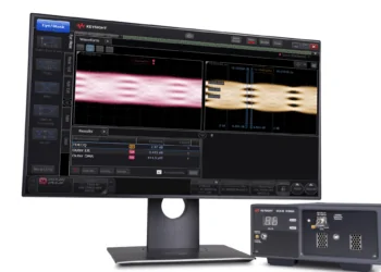
As silicon photonics moves into large-scale deployment for AI clusters, hyperscale data centers, optical interconnects, and co-packaged optics, engineers increasingly need to understand how a photonic device behaves within an end-to-end communication system before fabrication. Traditional workflows typically separate PIC design tools from optical system simulators, forcing engineers to move between environments and delaying system validation until later stages of development. Keysight’s ADS Photonic Designer now allows designers using GlobalFoundries’ silicon photonics platform to evaluate optical link performance metrics—including eye diagrams, signal integrity, and TDECQ (Transmitter and Dispersion Eye Closure Quaternary)—during the design process.
The integration also extends to Keysight’s FlexDCA oscilloscope software, helping engineers correlate simulation results with laboratory measurements during the development of optical transceivers, co-packaged optics, and next-generation optical interconnect architectures. The company says the workflow can accelerate time-to-first-design, reduce design-to-test discrepancies, and provide earlier visibility into system-level performance impacts.
- Supports GlobalFoundries silicon photonics process technology within ADS Photonic Designer
- Combines PIC design and EOE system simulation in a single workflow
- Enables simulation of eye diagrams, TDECQ, and optical link performance before tapeout
- Uses foundry-aligned, physics-based models correlated to fabricated silicon
- Integrates with Keysight FlexDCA software for improved simulation-to-measurement correlation
- Targets optical transceivers, co-packaged optics, AI infrastructure, and high-speed optical communications
- GlobalFoundries CLO PDK for ADS Photonic Designer is available immediately
Vikas Gupta, Senior Fellow, Silicon Photonics Product Line at GlobalFoundries, said: “As silicon photonics moves into broader deployment for AI infrastructure and high-speed optical communications, designers need workflows that connect device innovation with system-level performance from the start. By enabling our silicon photonics platform in Keysight’s ADS Photonic Designer, we’re helping customers accelerate development, reduce design risk and scale their optical interconnect solutions more effectively.”
🌐 Analysis: The announcement reflects a broader shift in the silicon photonics industry toward tighter integration between photonic device design, electronic design automation (EDA), and system-level modeling. As AI clusters scale toward hundreds of thousands of accelerators, the industry increasingly requires optical interconnects to be validated not only at the component level but also across complete communication channels. This has elevated the importance of photonic-aware EDA tools and foundry-supported PDK ecosystems.
GlobalFoundries continues to expand its silicon photonics strategy alongside growing demand for optical networking in AI infrastructure. Meanwhile, competitors including TSMC, Intel Foundry, Tower Semiconductor, and various specialized photonics foundries are advancing their own silicon photonics platforms. The ability to model co-packaged optics, linear-drive optics, and next-generation optical I/O architectures within unified simulation environments is becoming a key requirement for designers developing future AI networking systems.
🌐 We’re tracking the latest developments in networking silicon. Follow our ongoing coverage at: https://convergedigest.com/category/semiconductors/