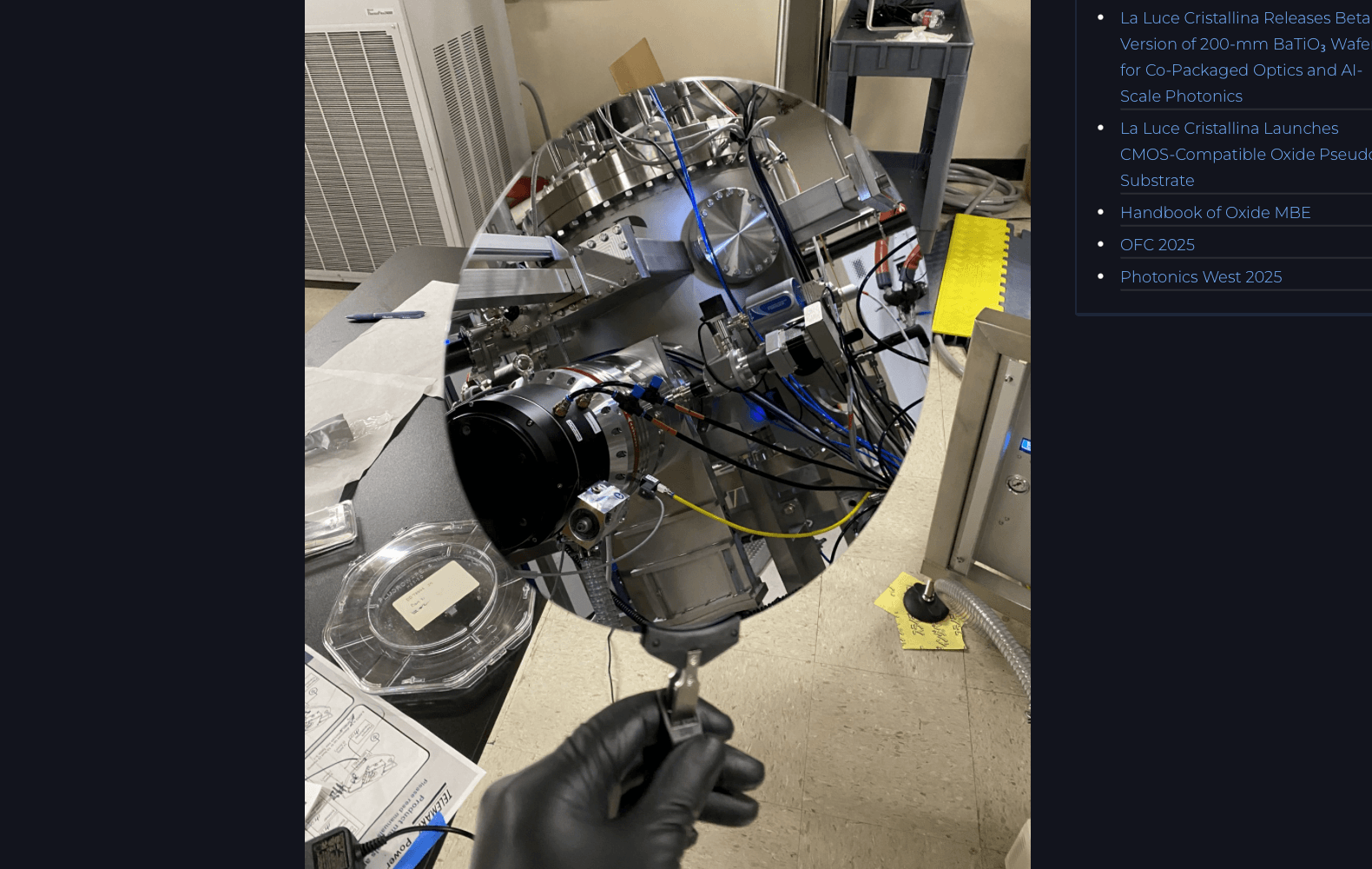
Austin-based La Luce Cristallina announced the beta availability of a 200-mm (8-inch) barium titanate (BaTiO₃) wafer platform designed for next-generation electro-optic modulators used in telecommunications and data communications systems. The company says the material platform targets ultra-low-voltage optical modulation, an important requirement for emerging co-packaged optics architectures supporting AI-scale data center infrastructure.
The BaTiO₃ wafers are engineered for integration into standard CMOS silicon manufacturing processes, allowing device makers to incorporate the material into existing silicon photonics fabrication flows without requiring major foundry retooling. The material’s very high Pockels coefficient—reaching roughly 1,300 pm/V in bulk single crystal form—enables electro-optic modulation at substantially lower drive voltages than conventional silicon photonics approaches. Lower modulation voltages reduce power consumption and simplify driver circuitry, key considerations as optical interconnect density increases inside AI clusters and hyperscale data centers.
La Luce Cristallina plans to demonstrate both its 200-mm and 50-mm (2-inch) BaTiO₃ wafers at the Optical Fiber Communication Conference (OFC) from March 17–19 at the Los Angeles Convention Center, booth 5507. The company positions the platform for a range of photonics applications beyond telecom interconnects, including quantum optical circuits, biosensing, LiDAR systems, and aerospace sensing technologies.
- Beta release of 200-mm (8-inch) BaTiO₃ wafers for electro-optic modulator development
- Designed for integration with standard CMOS silicon photonics manufacturing flows
- High Pockels coefficient (~1,300 pm/V) enables ultra-low-voltage optical modulation
- Targets applications in telecom, data communications, AI data centers, and quantum photonics
- Additional opportunities cited in biosensing, LiDAR, aerospace sensing, and field instrumentation
- Company will exhibit the wafers at OFC 2026, booth 5507 (West Hall)
“The beta version of our barium titanate wafer marks another step toward advancing co-packaged optics amid the rise of AI, quantum photonics and other high-capacity applications,” said Agham Posadas, CTO and co-founder of La Luce Cristallina. “With this beta version, current and prospective customers can test-drive our solution’s capabilities and unlock the full potential of barium titanate for powering multiple generations of electro-optic innovation across diverse use cases.”
🌐 Analysis
La Luce Cristallina focuses on integrating barium titanate (BaTiO₃) materials with silicon photonics platforms to enable high-performance electro-optic modulators. Unlike silicon modulators, which rely primarily on carrier-depletion or plasma dispersion effects, BaTiO₃ uses the Pockels effect—an intrinsic electro-optic property that allows very efficient modulation of light with extremely small applied voltages. By integrating BaTiO₃ films directly onto silicon wafers, the company aims to combine the scalability of CMOS manufacturing with the high electro-optic efficiency typically associated with materials such as lithium niobate. If manufacturable at scale on 200-mm wafers, this approach could significantly reduce modulator drive voltages and power consumption in silicon photonics transceivers.
The broader industry increasingly seeks new photonic materials to support higher-speed optical interconnects required by AI clusters. As data center networks transition toward co-packaged optics and tightly integrated photonic engines, modulator efficiency becomes critical because electrical I/O power and thermal limits increasingly constrain switch and accelerator packages. Materials such as BaTiO₃ could provide an alternative path alongside thin-film lithium niobate and emerging electro-optic polymers, enabling lower-voltage optical modulation directly integrated with CMOS photonics. Demonstrating scalable wafer-level manufacturing will determine whether BaTiO₃ can move from research platforms into high-volume optical interconnect products.