• Home
  • About
  • Events Calendar
  • Blueprint Guidelines
  • Privacy Policy
  • Manage Email Delivery
  • NextGenInfra.io
No Result
View All Result
Converge Digest
Tuesday, June 2, 2026
  • Home
  • About
  • Events Calendar
  • Blueprint Guidelines
  • Privacy Policy
  • Manage Email Delivery
  • NextGenInfra.io
No Result
View All Result
Converge Digest
No Result
View All Result

Home » Microchip Debuts 3 nm PCIe Gen 6 Switches

Microchip Debuts 3 nm PCIe Gen 6 Switches

October 15, 2025
in Semiconductors
A A

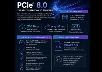
Microchip Technology has introduced its Switchtec Gen 6 PCIe switches, the industry’s first PCIe Gen 6 fanout switches built on a 3 nm process. Designed to meet the bandwidth and latency requirements of modern AI, HPC, and cloud infrastructures, the new devices deliver up to 160 lanes of PCIe 6.0 connectivity at 64 GT/s per lane—doubling the throughput of PCIe 5.0 while improving power efficiency and signal integrity.

The Switchtec Gen 6 family features advanced security capabilities, including a hardware root of trust, secure boot, and post-quantum-safe cryptography compliant with the U.S. Commercial National Security Algorithm Suite (CNSA) 2.0. The switches enable high-speed links among CPUs, GPUs, AI accelerators, and storage devices to prevent data transfer bottlenecks that can waste compute cycles. New protocol updates, such as Flow Control Unit (FLIT) mode and Forward Error Correction (FEC), further enhance reliability for AI workloads that rely on small, frequent data exchanges.

The 20-port, 10-stack switch architecture integrates an onboard MIPS processor, supports hot-plug capability, Non-Transparent Bridging (NTB), multicast for one-to-many data paths, and detailed diagnostics through Microchip’s ChipLink GUI tools. The PM61160-KIT evaluation platform and diagnostic suite enable developers to test and optimize connectivity designs quickly for hyperscale data center deployments. Sampling is now available for qualified customers.

• 3 nm process node with up to 160 PCIe 6.0 lanes at 64 GT/s

• Hardware root of trust and post-quantum-safe cryptography (CNSA 2.0 compliant)

• FLIT mode, dynamic resource allocation, and lightweight FEC for reduced latency

• 20 ports/10 stacks with x8 and x16 bifurcation options

• Integrated MIPS processor, NTB, multicast, and ChipLink diagnostics support

“By expanding our proven Switchtec product line to PCIe 6.0, we’re enabling this transformation with technology that facilitates direct communication between critical compute resources and delivers the most powerful and energy-efficient switch we’ve ever produced,” said Brian McCarson, corporate vice president of Microchip’s data center solutions business unit.

🌐 Analysis: Microchip’s entry into the PCIe 6.0 switch market underscores the growing need for ultra-low-latency interconnects in AI and HPC clusters. The use of 3 nm fabrication aligns it with the most advanced process technologies now being adopted by data center silicon suppliers. Competing PCIe 6.0 switch offerings are emerging from Broadcom and Microsemi divisions, while NVIDIA and AMD continue optimizing native interconnects through NVLink 5 and Infinity Fabric. Microchip’s approach positions it as a key supplier of flexible, standards-based connectivity for hyperscaler AI architectures.

🌐 We’re tracking the latest developments in networking silicon. Follow our ongoing coverage at: https://convergedigest.com/category/semiconductors/

ShareTweetShareSummarizeSummarize
Previous Post

QumulusAI Secures $500M Blockchain-Based Financing for GPUs 

Next Post

Infineon Drives 800V Power for AI Data Centers

Jim Carroll

Jim Carroll

Editor and Publisher, Converge! Network Digest, Optical Networks Daily - Covering the full stack of network convergence from Silicon Valley

Related Posts

All

Jeetu Patel: Cisco Silicon One, AI Agents, and the New Networking Supercycle

June 2, 2026
All

Chuck Robbins: AI Traffic Could Triple as Enterprises Modernize

June 2, 2026
All

Cisco Launches Cloud Control to Manage Infrastructure 

June 2, 2026
Subsea

Google and Telstra Partner on Australian Fibre and Subsea Infrastructure for the AI Era

June 2, 2026
All

Intel Targets the AI Inference Era with Rack-Scale Architecture

June 2, 2026
Screenshot
All

Lambda Evaluates NVIDIA Quantum-X Photonics CPO Switch

June 1, 2026
Next Post

Infineon Drives 800V Power for AI Data Centers

Categories

  • 5G / 6G / Wi-Fi
  • AI Infrastructure
  • All
  • Automotive Networking
  • Blueprints
  • Clouds and Carriers
  • Data Centers
  • Enterprise
  • Explainer
  • Feature
  • Financials
  • Last Mile / Middle Mile
  • Legal / Regulatory
  • Optical
  • Quantum
  • Research
  • Security
  • Semiconductors
  • Space
  • Start-ups
  • Subsea
  • Sustainability
  • Video
  • Webinars

Archives

Tags

5G All AT&T Australia AWS Blueprint columns BroadbandWireless Broadcom China Ciena Cisco Data Centers Dell'Oro Ericsson FCC Financial Financials Huawei Infinera Intel Japan Juniper Last Mile Last Mille LTE Mergers and Acquisitions Mobile NFV Nokia Optical Packet Systems PacketVoice People Regulatory Satellite SDN Service Providers Silicon Silicon Valley StandardsWatch Storage TTP UK Verizon Wi-Fi
Converge Digest

A private dossier for networking and telecoms

Follow Us

  • Home
  • About
  • Events Calendar
  • Blueprint Guidelines
  • Privacy Policy
  • Manage Email Delivery
  • NextGenInfra.io

© 2026 Converge Digest - A private dossier for networking and telecoms.

No Result
View All Result
  • Home
  • About
  • Events Calendar
  • Blueprint Guidelines
  • Privacy Policy
  • Manage Email Delivery
  • NextGenInfra.io

© 2026 Converge Digest - A private dossier for networking and telecoms.

This website uses cookies. By continuing to use this website you are giving consent to cookies being used. Visit our Privacy and Cookie Policy.
Go to mobile version