MultiLane has achieved reliable 120 GHz high-frequency performance on standard PCB technology, proving that 448G PAM4-class interconnects can be built without premium laminates or exotic fabrication. The company’s new footprint architecture improves PCB transition behavior across its SMPX multiport and RF Precision 1.00 mm ecosystems, countering the long-held assumption that millimeter-wave operation requires costly materials. This establishes a practical path toward commercially viable 200G/lane and 448G designs as data center and semiconductor developers push into the next speed tier.
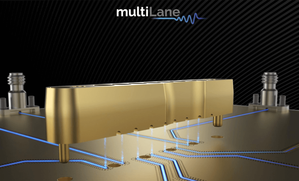
The breakthrough directly addresses the PCB transition bottleneck that has historically limited system performance above 100 GHz, even when connectors themselves support higher frequencies. MultiLane applied systematic electromagnetic design and layout refinement to standard PCB processes—typically aimed at 50–70 GHz operation—and extended usable bandwidth to 110 GHz with clean S-parameters, validated through 120 GHz across multiple channels and board revisions. Testing combined SMPX multiport launches, 1.00 mm vertical connectors, and SMPX-to-1.00 mm cable assemblies to confirm low insertion loss and consistent return loss across the full chain.
This engineering-driven approach now benefits both dense SMPX multiport systems and the RF Precision 1.00 mm ecosystem, reducing cost and complexity for developers targeting next-generation test systems and 448G interconnect architectures. By demonstrating that footprint architecture—not laminate class—is the true limiter, MultiLane provides a scalable route for OEMs to build future 100 GHz+ platforms with wider manufacturability and predictable performance.
Highlights
- Achieves stable PCB transition performance beyond 110 GHz, validated at 120 GHz for 448G PAM4 operation.
- Uses standard PCB manufacturing processes rather than premium, millimeter-wave-grade laminates.
- Improves conductor symmetry, launch geometry, and transition design using systematic engineering rather than materials-driven approaches.
- Applies across both SMPX multiport systems and RF Precision 1.00 mm connectors, jumpers, adapters, and terminators.
- VNA testing confirmed repeatable S-parameters across multiple channels and board builds.
- Enables cost-effective development of 200G/lane and 448G-class platforms.
- Reduces validation complexity by removing PCB transitions as the system bottleneck.
“By focusing on intelligent footprint engineering rather than exotic materials, we’ve shown that ultra-high-frequency PCB transitions can be both high-performing and cost-effective,” the company stated.
https://www.multilaneinc.com/resources/Articles/Entering%20the%20448G%20Era.pdf
🌐 Analysis
MultiLane’s accomplishment aligns with growing industry momentum around OIF CEI-224G/448G and IEEE 802.3dj as developers push toward 200G/lane electrical signaling. The ability to test and interconnect at 100–120 GHz using standard PCB processes lowers barriers for switch, optics, and test vendors preparing next-generation platforms. Competitors pursuing similar high-frequency validation will likely evaluate materials-versus-architecture tradeoffs as industry demand accelerates.