At the OIF’s 448Gbps Signaling for AI Workshop in Santa Clara , Google’s Tad Hofmeister, Optical Hardware Engineer for Machine Learning Systems, made a compelling case for rapid industry alignment on next-generation SerDes technologies. With AI workloads scaling at breakneck speed, Hofmeister emphasized the need to push beyond the limits of 224G lanes and begin deploying 448G in both scale-up and scale-out AI network fabrics.
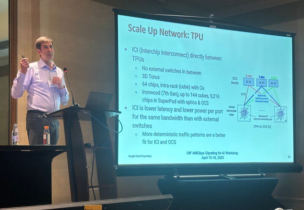
Google’s latest TPU generation, codenamed Ironwood, and the company’s GE200-based GPU clusters, are pushing the envelope on performance and bandwidth demands. Hofmeister noted that while copper interconnects are still viable for short-reach intra-rack topologies, optical links are essential for scaling across multi-rack AI superpods. Google’s use of a proprietary ICI protocol for TPU interconnects—with optical circuit switches between pods—underscores the importance of flexible, high-capacity networking architectures.
Hofmeister also addressed challenges in connector design, channel integrity, and power tradeoffs. He suggested the industry may need to abandon backward compatibility in OSFP connectors and coalesce around either PAM6 or PAM8 signaling to move forward efficiently. Flyover cables and co-packaged copper are seen as necessary enablers to bypass traditional PCB limitations.
Key Takeaways:
- Google advocates urgent industry focus on 448G SerDes for AI workloads.
- TPU superpods interconnect up to 9,216 chips via a proprietary ICI protocol and optical circuit switches.
- OSFP module limitations likely necessitate a new connector design without backward compatibility.
- Co-packaged copper and flyover cables are critical to signal integrity at 448G.
- Google sees PAM4 as insufficient; PAM6 or PAM8 are more realistic paths.
“We’re not just looking for lower power or cost—we’re out of escape lanes. 224G is hitting its limits, and enabling 448G is now essential to keep scaling AI compute. Let’s narrow the scope and get it done.”
— Tad Hofmeister, Optical Hardware Engineer, Google Cloud