• Home
  • About
  • Events Calendar
  • Blueprint Guidelines
  • Privacy Policy
  • Manage Email Delivery
  • NextGenInfra.io
  • buzzwords
  • Archives
  • Milestones
  • On This Day
  • Video Search
Converge Digest
Wednesday, July 15, 2026
  • Home
  • About
  • Events Calendar
  • Blueprint Guidelines
  • Privacy Policy
  • Manage Email Delivery
  • NextGenInfra.io
  • buzzwords
  • Archives
  • Milestones
  • On This Day
  • Video Search
No Result
View All Result
Converge Digest
No Result
View All Result

Home » Samsung updates roadmap, aims for 1.4nm nodes in 2027

Samsung updates roadmap, aims for 1.4nm nodes in 2027

October 3, 2022
in Semiconductors
A A

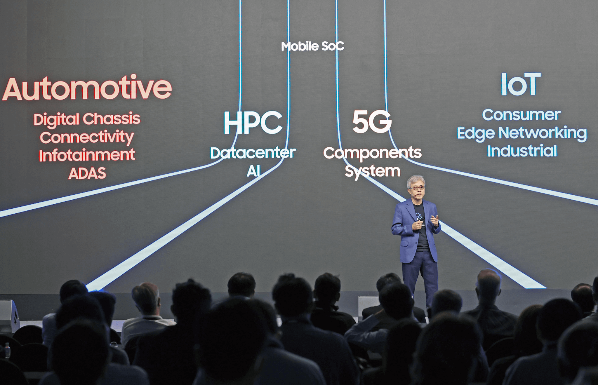
At its annual Samsung Foundry Forum event in San Jose, California, Samsung Electronics outlined its goals to drive process nodes to 1.4nm in 2027. 

Samsung, which currently has 3nm process technology in mass production, Samsung will be further enhancing gate-all-around (GAA) based technology and plans to introduce the 2nm process in 2025 and 1.4nm process in 2027.

The event focused on foundry process technology innovation, process technology optimization for each specific applications, stable production capabilities, and customized services, including the enhancement its GAA-based 3nm process support for HPC and mobile applications. Samsung will also diversify the 4nm process for HPC and automotive applications.

For automotive customers specifically, Samsung is currently providing embedded non-volatile memory (eNVM) solutions based on 28nm technology. In order to support automotive-grade reliability, the company plans to further expand process nodes by launching 14nm eNVM solutions in 2024 and adding 8nm eNVM in the future. Samsung has been mass producing 8nm RF following 14nm RF, and 5nm RF is currently in development.

“The technology development goal down to 1.4nm and foundry platforms specialized for each application, together with stable supply through consistent investment are all part of Samsung’s strategies to secure customers’ trust and support their success,” said Dr. Si-young Choi, president and head of Foundry Business at Samsung Electronics. “Realizing every customer’s innovations with our partners has been at the core of our foundry service.”

Samsung also confirmed that its 3D packaging X-Cube with micro-bump interconnection will be ready for mass production in 2024, and bump-less X-Cube will be available in 2026.

In addition, Samsung highlighted its production expansion. The company plans to expand its production capacity for the advanced nodes by more than three times by 2027 compared to this year. Including the new fab under construction in Taylor, Texas, Samsung’s foundry manufacturing lines are currently in five locations: Giheung, Hwaseong, and Pyeongtaek in Korea; and Austin and Taylor in the United States.

https://news.samsung.com/global/samsung-electronics-unveils-plans-for-1-4nm-process-technology-and-investment-for-production-capacity-at-samsung-foundry-forum-2022

Tags: SamsungSilicon
ShareTweetShareSummarizeSummarize
Previous Post

Lockheed Martin and Verizon demo 5G.MIL drones

Next Post

Wind River teams with Tata Consultancy on vRAN

Staff

Staff

Related Posts

5G / 6G / Wi-Fi

Samsung AI RAN Optimizer Boosts KDDI 5G Throughput by Up to 52%

July 6, 2026
AI Infrastructure

South Korea Unveils National AI Infrastructure Strategy 

June 29, 2026
All

Samsung’s UFS 5.0 Doubles Storage Performance for AI Smartphones

June 26, 2026
5G / 6G / Wi-Fi

Broadcom and Samsung Link 5G Release 17 Modem with Wi-Fi 8

May 27, 2026
Enterprise

KKR Invests $820 Million in Samsung SDS

April 14, 2026
Space Networking & Orbital Data Centers

Keysight, Samsung Showcase NR-NTN LEO Mobility Testing 

February 5, 2026
Next Post

Wind River teams with Tata Consultancy on vRAN

Please login to join discussion

Categories

  • 5G / 6G / Wi-Fi
  • AI Infrastructure
  • All
  • Automotive Networking
  • Blueprints
  • Clouds and Carriers
  • Corporate Strategies
  • CPO
  • Data Centers
  • Enterprise
  • Explainer
  • Feature
  • Hot Start-ups
  • Last Mile / Middle Mile
  • Legal / Regulatory
  • Optical
  • Optical I/O
  • Pluggable Optics
  • Quantum
  • Research
  • Security
  • Semiconductors
  • Silicon Photonics
  • Space Networking & Orbital Data Centers
  • Subsea
  • Sustainability
  • Video
  • Webinars
Converge Digest

A private dossier for networking and telecoms

Follow Us

  • Home
  • About
  • Events Calendar
  • Blueprint Guidelines
  • Privacy Policy
  • Manage Email Delivery
  • NextGenInfra.io
  • buzzwords
  • Archives
  • Milestones
  • On This Day
  • Video Search

© 2026 Converge Digest - A private dossier for networking and telecoms.

No Result
View All Result
  • Home
  • About
  • Events Calendar
  • Blueprint Guidelines
  • Privacy Policy
  • Manage Email Delivery
  • NextGenInfra.io
  • buzzwords
  • Archives
  • Milestones
  • On This Day
  • Video Search

© 2026 Converge Digest - A private dossier for networking and telecoms.

This website uses cookies. By continuing to use this website you are giving consent to cookies being used. Visit our Privacy and Cookie Policy.
Go to mobile version