• Home
  • About
  • Events Calendar
  • Blueprint Guidelines
  • Privacy Policy
  • Manage Email Delivery
  • NextGenInfra.io
  • buzzwords
  • Archives
  • Milestones
  • On This Day
  • Video Search
Converge Digest
Tuesday, July 14, 2026
  • Home
  • About
  • Events Calendar
  • Blueprint Guidelines
  • Privacy Policy
  • Manage Email Delivery
  • NextGenInfra.io
  • buzzwords
  • Archives
  • Milestones
  • On This Day
  • Video Search
No Result
View All Result
Converge Digest
No Result
View All Result

Home » SK hynix previews 321-layer 4D NAND

SK hynix previews 321-layer 4D NAND

August 9, 2023
in Semiconductors
A A

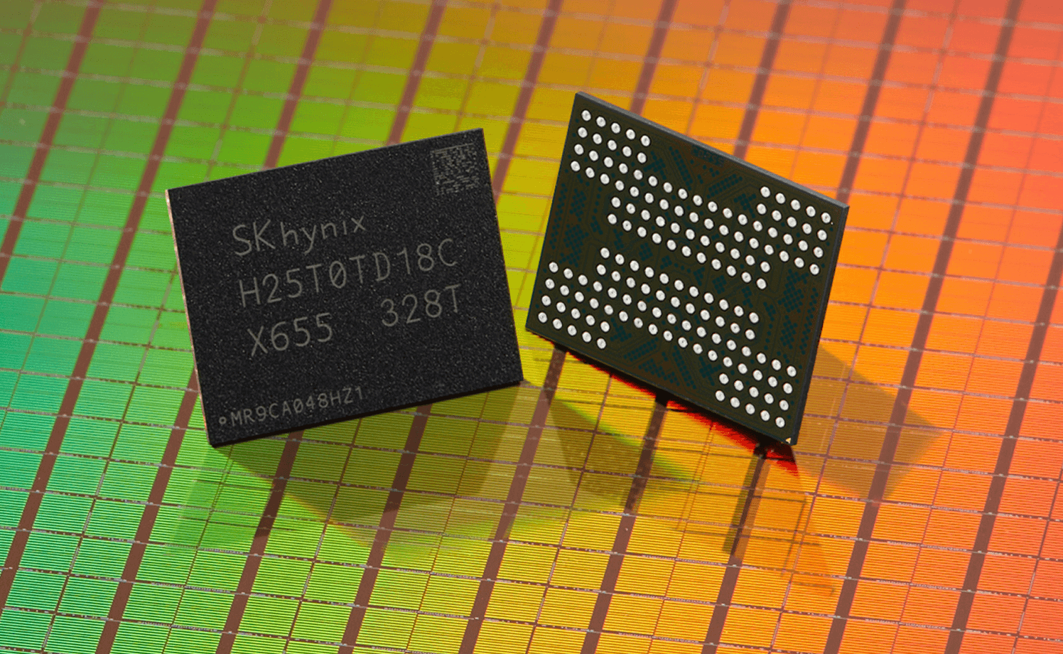
SK hynix previewed samples of its 321-layer 4D NAND at this week’s Flash Memory Summit (FMS) 2023 in Santa Clara, California. The company plans to raise the level of completion of the 321-layer product and start mass production from the first half of 2025.

The device is the first NAND memory to exceed 300 layers.

SK hynix expects its 321-layer 1Tb TLC NAND comes will bring a 59% improvement in productivity, compared with the earlier generation of 238-layer 512Gb, thanks to the technology development that enabled stacking of more cells and larger storage capacity on a single chip, meaning the total capacity that can be produced on a single wafer increased.

SK hynix also announced that it has started development of the next-generation PCIe Gen6 and UFS 5.0.


Tags: MemorySk HynixStorage
ShareTweetShareSummarizeSummarize
Previous Post

Dell’Oro: Service Provider router market to hit $77B over 5 years

Next Post

Cignal AI: Linear optics and 800G optics forecast

Jim Carroll

Jim Carroll

Editor and Publisher, Converge! Network Digest, Optical Networks Daily - Covering the full stack of network convergence from Silicon Valley

Related Posts

Screenshot
Corporate Strategies

SK Hynix Raises $26.5 Billion as AI Memory Demand Drives U.S. Listing

July 10, 2026
AI Infrastructure

South Korea Unveils National AI Infrastructure Strategy 

June 29, 2026
Semiconductors

Argonne Leads DOE-Funded Project to Pioneer Extreme-Scale Memory

January 11, 2025
Semiconductors

Alphawave demos 9.2 Gbps HBM3E, 1.2 TBps memory bandwidth

June 20, 2024
Semiconductors

SK hynix to build $3.8B advanced packaging fab in Indiana

April 4, 2024
Semiconductors

Rambus unveils 9.6 Gbps HBM3 Memory Controller IP

October 25, 2023
Next Post

Cignal AI: Linear optics and 800G optics forecast

Categories

  • 5G / 6G / Wi-Fi
  • AI Infrastructure
  • All
  • Automotive Networking
  • Blueprints
  • Clouds and Carriers
  • Corporate Strategies
  • CPO
  • Data Centers
  • Enterprise
  • Explainer
  • Feature
  • Hot Start-ups
  • Last Mile / Middle Mile
  • Legal / Regulatory
  • Optical
  • Optical I/O
  • Pluggable Optics
  • Quantum
  • Research
  • Security
  • Semiconductors
  • Silicon Photonics
  • Space Networking & Orbital Data Centers
  • Subsea
  • Sustainability
  • Video
  • Webinars
Converge Digest

A private dossier for networking and telecoms

Follow Us

  • Home
  • About
  • Events Calendar
  • Blueprint Guidelines
  • Privacy Policy
  • Manage Email Delivery
  • NextGenInfra.io
  • buzzwords
  • Archives
  • Milestones
  • On This Day
  • Video Search

© 2026 Converge Digest - A private dossier for networking and telecoms.

No Result
View All Result
  • Home
  • About
  • Events Calendar
  • Blueprint Guidelines
  • Privacy Policy
  • Manage Email Delivery
  • NextGenInfra.io
  • buzzwords
  • Archives
  • Milestones
  • On This Day
  • Video Search

© 2026 Converge Digest - A private dossier for networking and telecoms.

This website uses cookies. By continuing to use this website you are giving consent to cookies being used. Visit our Privacy and Cookie Policy.
Go to mobile version