The U.S. Department of Commerce has launched a new initiative under the CHIPS for America program, designed to strengthen domestic semiconductor manufacturing capabilities through advanced packaging technologies. Administered by the National Institute of Standards and Technology (NIST), the National Advanced Packaging Manufacturing Program (NAPMP) is offering up to $1.55 billion in funding over five years to support research and development (R&D) in critical areas. The initiative focuses on five key R&D domains: equipment, tools, processes, and integration; power delivery and thermal management; connector technologies including photonics and radio frequency (RF); chiplet ecosystems; and co-design/electronic design automation (EDA). Applications for concept papers must be submitted by December 20, 2024.
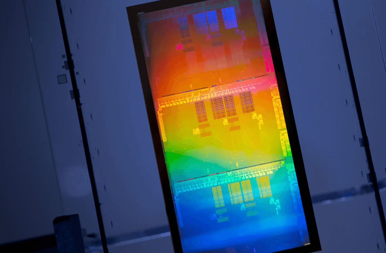
The NAPMP aims to position the U.S. as a global leader in advanced semiconductor packaging technologies, which are essential for emerging fields such as high-performance computing, artificial intelligence (AI), and low-power electronics. With the growing demand for more sophisticated and efficient semiconductor designs, advanced packaging is crucial for improving performance and reducing power consumption. This program seeks to establish a sustainable, domestic packaging industry that can handle advanced-node chips manufactured both in the U.S. and abroad. NIST expects the program to also spur innovation in packaging design and architectures, while fostering the growth of a highly skilled workforce capable of supporting the sector’s long-term success.
Eligible applicants for the funding include domestic for-profit organizations, non-profits, accredited institutions of higher education, and state, local, and tribal governments. The NAPMP is designed to facilitate collaboration among industry leaders, academic institutions, and research centers. Selected projects will focus on prototyping and advancing semiconductor packaging technologies such as photonics and RF, areas critical for the future of AI and other high-demand applications. As part of the broader CHIPS for America initiative, this funding opportunity will play a vital role in enhancing the U.S. semiconductor industry’s competitive edge. “This program will accelerate innovation in semiconductor packaging and provide a foundation for future technological advancements,” stated a NIST spokesperson.
- The five R&D areas are:
- Equipment, tools, processes, and process integration
- Power delivery and thermal management
- Connector technology, including photonics and radio frequency (RF)
- Chiplets ecosystem
- Co-design/electronic design automation (EDA)
Key Points:
• Up to $1.55 billion in funding available over five years for semiconductor advanced packaging R&D.
• Five key R&D areas: equipment, tools, processes, and integration; power delivery and thermal management; connector technologies (including photonics and RF); chiplet ecosystems; and co-design/EDA.
• Applications for concept papers due by December 20, 2024, with full applications due 60 days after an invitation.
• Eligible applicants include U.S.-based for-profit organizations, non-profits, educational institutions, and government entities.
• Individual awards expected to range from $10M to $150M per project, with an emphasis on prototyping and collaboration between industry and academia.