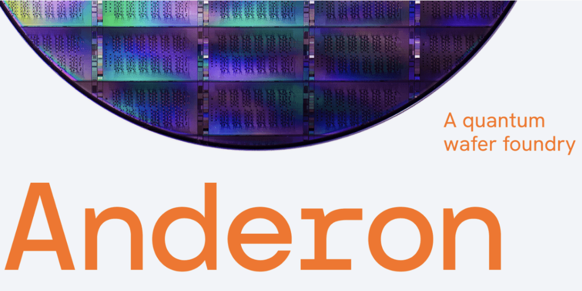
IBM and the U.S. Department of Commerce signed a Letter of Intent to support Anderon, a new IBM-backed standalone company that aims to operate America’s first pure-play quantum chip foundry. The proposed Albany, New York-based company would focus on 300-millimeter quantum wafer fabrication and serve IBM and other quantum hardware vendors.
The plan includes up to $1 billion in CHIPS R&D incentives from the Department of Commerce and a matching $1 billion cash contribution from IBM. IBM also plans to contribute intellectual property, assets, fabrication expertise, and a skilled workforce. The agreement remains subject to negotiation and execution of definitive documents.
Anderon will initially support superconducting qubit wafers and related electronics, with plans to expand into other quantum modalities. Its planned process capabilities include superconducting wiring, through-silicon vias, bumps, process design kits, in-line wafer testing, characterization, and baseline fabrication routes designed for rapid hardware iteration. IBM said the foundry initiative builds on decades of quantum research, semiconductor manufacturing expertise, and collaborations with U.S. government agencies including NIST, DARPA, and Department of Energy laboratories.
• New company: Anderon
• Parent/backer: IBM
• Government partner: U.S. Department of Commerce
• Planned location: Albany, New York
• Facility type: 300-millimeter quantum wafer foundry
• CHIPS incentive: $1 billion
• IBM cash contribution: $1 billion
• Initial focus: superconducting qubits and supporting electronics
• Broader goal: U.S.-based quantum wafer manufacturing for multiple vendors
“IBM has pioneered quantum computing for decades. Our work in silicon wafer fabrication has been a key to IBM’s success and will be critical to enable a broader quantum technology landscape that will reshape global innovation and economic competitiveness,” said Arvind Krishna, Chairman and CEO of IBM. “With the support of the U.S. Department of Commerce, Anderon will be well-positioned to fuel America’s fast-growing quantum technology industry.”
🌐 Analysis
The Anderon initiative extends IBM’s long-term strategy to control the full quantum computing stack — from chip fabrication and cryogenic hardware to middleware, cloud delivery, and application development. Unlike many quantum startups that focus on a single qubit modality or subsystem, IBM has steadily built an integrated quantum platform that combines superconducting processors, software tooling, packaging, calibration, orchestration, and cloud accessibility.
IBM’s earliest quantum efforts emerged from its superconducting qubit research program, where the company leveraged decades of expertise in low-temperature physics, semiconductor processing, and advanced packaging. The company chose superconducting transmon qubits as its primary architecture, relying on microwave-controlled Josephson junction circuits fabricated on silicon wafers. This approach aligned naturally with IBM’s semiconductor manufacturing heritage and enabled the company to scale quantum processors using increasingly advanced lithography, packaging, and interconnect technologies.
A major inflection point came in 2016 when IBM launched the IBM Quantum Experience, providing public cloud access to a superconducting quantum processor. That move accelerated the development of the modern quantum software ecosystem by giving researchers, universities, enterprises, and developers direct access to real hardware. IBM subsequently built Qiskit into one of the most widely adopted quantum software development frameworks in the industry.
IBM’s roadmap later evolved from small experimental processors into progressively larger systems such as Falcon, Hummingbird, Eagle, Osprey, Condor, and Heron. In parallel, IBM focused heavily on error mitigation, cryogenic integration, and modular quantum system architecture. The company introduced IBM Quantum System One as an integrated commercial quantum computing platform and later unveiled Quantum System Two, designed as a modular architecture capable of networking multiple quantum processors together inside a larger computational fabric.
Heron represented a particularly important milestone because IBM shifted emphasis away from simply increasing qubit counts toward improving gate fidelity, reducing crosstalk, and enabling utility-scale quantum circuits. IBM has increasingly argued that quantum performance depends on error suppression and system engineering rather than raw qubit scaling alone.
The company’s current roadmap targets large-scale fault tolerance later this decade. IBM has outlined plans for “Starling,” a system expected to support approximately 200 logical qubits and execute up to 100 million quantum gates by 2029. Achieving that objective depends not only on qubit design but also on advanced wafer manufacturing, multilayer integration, superconducting interconnects, packaging density, and highly repeatable fabrication processes.
That requirement helps explain the strategic importance of Anderon. The initiative attempts to move quantum hardware manufacturing closer to a semiconductor foundry model, where repeatable 300mm wafer processing, process design kits, inline metrology, and supply chain standardization become central to scaling production. If successful, Anderon could help establish a domestic manufacturing base for superconducting quantum hardware while also supporting other quantum hardware vendors that need specialized fabrication capabilities unavailable through conventional semiconductor foundries.
The broader competitive backdrop is also shifting rapidly. Google, Microsoft, Amazon Web Services, Intel, Quantinuum, IonQ, Rigetti, PsiQuantum, Atom Computing, Xanadu, and several national laboratories continue pursuing competing quantum architectures, including trapped ions, neutral atoms, photonics, silicon spin qubits, and topological approaches. IBM’s strategy differs in that it combines open software ecosystems, deployed quantum cloud infrastructure, and vertically integrated manufacturing under a single long-term roadmap.
| Year | IBM Quantum Milestone | Core Technology / Significance |
|---|---|---|
| 2016 | IBM Quantum Experience launched | First public cloud access to superconducting quantum hardware; helped catalyze the global quantum developer ecosystem. |
| 2017 | Commercial IBM Q program introduced | Enterprise and research access model for quantum systems and software development. |
| 2019 | IBM Quantum System One unveiled | Integrated commercial quantum computing platform combining cryogenics, control systems, and superconducting processors. |
| 2020 | 127-qubit Eagle roadmap announced | Transition toward larger-scale superconducting processors using advanced multilayer integration. |
| 2021 | Eagle processor introduced | 127-qubit superconducting processor using improved wiring density and packaging architecture. |
| 2022 | 433-qubit Osprey processor launched | Expanded qubit scaling with increased focus on calibration and coherence management. |
| 2023 | Quantum System Two and Heron announced | Modular quantum-centric supercomputing architecture emphasizing higher fidelity and lower crosstalk. |
| 2024 | Fault-tolerant roadmap refinement | Shift toward logical qubits, error correction, and scalable quantum orchestration. |
| 2025 | Expanded global deployment footprint | IBM surpassed 90 deployed quantum systems globally and expanded partnerships across industry and government. |
| 2026 | Anderon quantum foundry initiative announced | 300mm quantum wafer foundry targeting superconducting qubits, advanced packaging, TSVs, superconducting wiring, and scalable U.S.-based manufacturing. |
| 2029 target | IBM Starling roadmap target | Projected fault-tolerant quantum system with approximately 200 logical qubits and 100 million quantum gates. |