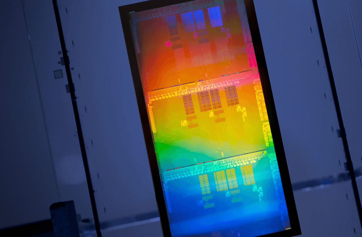
AMD said it will invest more than $10 billion across Taiwan’s semiconductor ecosystem to expand strategic partnerships and scale advanced packaging capacity for next-generation AI infrastructure. The announcement underscores the company’s growing dependence on Taiwan not only for leading-edge wafer production, but also for advanced packaging, substrates, assembly, and system integration as AI cluster deployments move toward rack-scale and multi-gigawatt scale.
At the center of the initiative is AMD’s work on Elevated Fanout Bridge (EFB), a next-generation 2.5D packaging technology designed to increase die-to-die interconnect bandwidth while improving power efficiency. AMD said EFB will play a role in its 6th Gen EPYC processors, code-named “Venice,” enabling denser chiplet integration and higher performance-per-watt. AMD is collaborating with ASE Technology and Siliconware Precision Industries to industrialize wafer-based EFB, while working with PTI on what it says is the industry’s first qualified 2.5D panel-based EFB interconnect. The move reflects broader industry momentum toward more advanced packaging architectures as conventional scaling increasingly depends on interconnect and packaging innovation.
AMD said these manufacturing advances will support production of its upcoming AMD Helios rack-scale AI platform, expected to enter deployment in the second half of 2026. Helios combines “Venice” CPUs with AMD Instinct MI450X GPUs, advanced networking, and the ROCm software stack. Manufacturing partners including Sanmina, Wiwynn, Wistron and Inventec are supporting system assembly, while substrate suppliers including Unimicron, Nan Ya PCB and Kinsus are contributing to the broader supply chain.
- AMD will invest more than $10 billion across Taiwan’s chip manufacturing and packaging ecosystem.
- Focus areas include advanced packaging, 2.5D EFB interconnects, substrates, and system integration.
- EFB packaging is expected to support 6th Gen AMD EPYC “Venice” processors with higher bandwidth and improved efficiency.
- The initiative supports manufacturing ramp for the AMD Helios rack-scale AI platform.
- Helios deployments with MI450X GPUs and Venice CPUs remain on track for 2H 2026.
- Taiwan partners named include ASE, SPIL, PTI, Unimicron, Nan Ya PCB, Kinsus, Wiwynn, Wistron, Inventec, Sanmina, and AIC.
“By combining AMD leadership in high-performance computing with the Taiwan ecosystem and our strategic global partners, we are enabling integrated, rack-scale AI infrastructure that helps customers accelerate deployment of next-generation AI systems,” said Dr. Lisa Su, Chair and CEO of AMD.
🌐 Analysis
AMD’s announcement highlights how advanced packaging has become one of the most strategic battlegrounds in AI infrastructure. Performance gains in AI servers increasingly depend on chiplet integration, HBM attachment, substrate technology, and high-density interconnects—not just smaller process nodes. AMD has emphasized chiplet architecture for several product generations, but this investment signals a deeper effort to secure packaging scale ahead of large Helios deployments and anticipated demand for MI450X-based AI clusters.
The move also reinforces Taiwan’s central role in the global AI hardware supply chain. While NVIDIA, Intel and AMD continue to compete on accelerator performance, they increasingly rely on the same Taiwan-based ecosystem for advanced packaging, substrates and assembly capacity. For AMD, locking in that capacity early could be critical as hyperscalers prepare for multi-gigawatt AI infrastructure buildouts beginning later this year.
Addendum: What is AMD’s Elevated Fanout Bridge (EFB)?
AMD’s Elevated Fanout Bridge (EFB) is an advanced 2.5D packaging technology that connects multiple chiplets using localized, high-density silicon bridges rather than a single, massive silicon interposer spanning the entire package. By embedding these tiny bridges directly into the organic packaging layers only where chiplets interface, EFB delivers ultra-high die-to-die bandwidth while drastically reducing manufacturing costs and enabling larger, more complex package sizes for AI and high-performance computing (HPC).
In traditional 2.5D packaging, all dies sit atop a large monolithic silicon floor to route signals between compute chiplets and High-Bandwidth Memory (HBM). EFB sidesteps this requirement, utilizing small bridge structures to drastically cut the amount of specialized silicon needed inside the package. This preserves short electrical paths between adjacent dies, resulting in lower power consumption for data movement, excellent signal integrity, and greater modular flexibility.
This technology is vital as AI accelerators and server CPUs scale past traditional manufacturing size limits. AMD has confirmed EFB’s deployment in its 6th Gen EPYC “Venice” processors and its broader Helios rack-scale AI platform. By co-developing and scaling this technology with global packaging partners—including ASE, SPIL, and PTI—AMD is positioning EFB as a highly scalable, high-yield alternative to industry capacity bottlenecks.
Profile: AMD Elevated Fanout Bridge (EFB)
| Technology | Advanced 2.5D chiplet packaging with localized bridge interconnects |
| Primary Purpose | High-bandwidth die-to-die interconnect for AI processors and server CPUs |
| Key Benefit | Reduces reliance on large monolithic silicon interposers while maintaining dense chiplet connectivity |
| Bandwidth Goal | Very high die-to-die bandwidth for chiplet communication and memory integration |
| Efficiency Advantage | Shorter electrical paths can improve signal integrity and performance-per-watt |
| Manufacturing Advantage | Supports broader OSAT ecosystem scaling beyond a single packaging supplier |
| AMD Products | 6th Gen AMD EPYC “Venice”; AMD Helios AI platform |
| Ecosystem Partners | ASE, SPIL, PTI and additional Taiwan advanced packaging partners |
| Strategic Importance | Helps AMD scale next-generation AI infrastructure amid strong demand for advanced packaging capacity |
For Further Reference: AMD Advanced Packaging and Elevated Fanout Bridge (EFB)
| AMD Chiplet Architecture White Paper | AMD overview of chiplet-based design, heterogeneous integration, die partitioning and packaging evolution across EPYC and Instinct platforms. View White Paper → |
| AMD CDNA 4 Architecture White Paper | Technical overview of AMD’s AI GPU architecture, including advanced packaging, HBM integration, chiplet connectivity and accelerator scaling. View White Paper → |
| AMD CDNA Architecture Overview | AMD resource page covering CDNA accelerator architecture, packaging technologies, software stack and AI infrastructure positioning. Visit AMD CDNA Overview → |
| Engineering the Future of AI | AMD engineering blog discussing AI interconnects, Infinity Fabric, packaging innovation and rack-scale AI infrastructure. Read AMD Blog → |
| AMD 2025 Financial Analyst Day | AMD corporate strategy presentation outlining future compute roadmap, AI systems, packaging innovation and ecosystem partnerships. View Presentation → |
| AMD 3D V-Cache Technology | Background on AMD’s broader advanced packaging innovations including 3D stacking, die bonding and memory integration technologies relevant to future AI processor packaging. Learn More → |
🌐 We’re tracking the latest developments in networking silicon. Follow our ongoing coverage at: https://convergedigest.com/category/semiconductors/