• Home
  • About
  • Events Calendar
  • Blueprint Guidelines
  • Privacy Policy
  • Manage Email Delivery
  • NextGenInfra.io
No Result
View All Result
Converge Digest
Thursday, June 11, 2026
  • Home
  • About
  • Events Calendar
  • Blueprint Guidelines
  • Privacy Policy
  • Manage Email Delivery
  • NextGenInfra.io
No Result
View All Result
Converge Digest
No Result
View All Result

Home » Applied Materials Targets 2nm with Hybrid Bonding, GAA Epi, and eBeam 

Applied Materials Targets 2nm with Hybrid Bonding, GAA Epi, and eBeam 

October 7, 2025
in All
A A

Applied Materials has unveiled three new semiconductor manufacturing platforms designed to advance chip performance, power efficiency, and yield for next-generation AI and high-performance computing (HPC) devices. The company’s new Kinex, Xtera, and PROVision 10 systems target key areas of the semiconductor stack—advanced packaging, transistor architecture, and metrology—aimed squarely at enabling 2nm and beyond chip production.

The Kinex™ Bonding System, co-developed with BE Semiconductor Industries (Besi), integrates all critical steps of die-to-wafer hybrid bonding into one tool. Hybrid bonding directly connects copper pads between dies, eliminating solder bumps and reducing interconnect resistance and power loss. By merging Applied’s front-end wafer processing with Besi’s precision die placement, Kinex enables sub-micron alignment accuracy, faster drift detection, and clean, low-defect environments essential for chiplet-based GPUs, CPUs, and HBM packages.

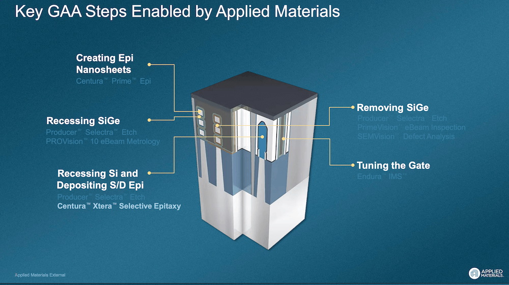
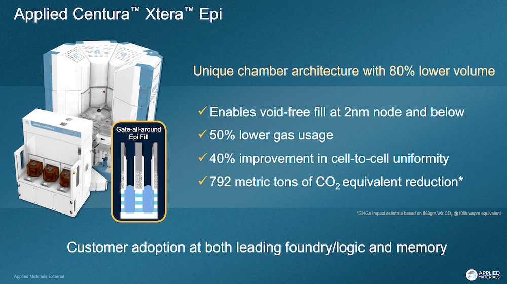
The Centura™ Xtera™ Epi System focuses on fabricating high-performance Gate-All-Around (GAA) transistors at 2nm nodes and smaller. Traditional epitaxial growth can leave voids in deep transistor trenches, degrading reliability. Xtera solves this with a continuous deposition-etch cycle that dynamically widens trenches as material grows, ensuring uniform, void-free epitaxial layers while cutting gas usage by 50%. The result is improved uniformity across billions of nanosheet transistors.

The PROVision™ 10 eBeam Metrology System pushes process control further into the 3D realm. Using cold field emission (CFE) technology, it achieves up to 50% higher image resolution and 10x faster imaging than previous thermal systems. It enables sub-nanometer imaging across multiple layers, detecting nanosheet variations, EUV overlay shifts, and voids in 3D transistors—all vital for yield enhancement in GAA logic and next-generation DRAM and NAND designs.

“Applied is focused on driving materials engineering breakthroughs to provide the performance and power-efficiency improvements needed to scale AI,” said Dr. Prabu Raja, President of the Semiconductor Products Group at Applied Materials.

🌐 Analysis:

This launch underscores Applied Materials’ dominance in the materials engineering domain as the semiconductor industry transitions to 2nm-class and chiplet-based architectures. Hybrid bonding (Kinex) and GAA epitaxy (Xtera) are foundational for next-generation GPU and HBM manufacturing, directly affecting AI chip performance and power efficiency. The PROVision 10 system addresses a growing need for ultra-precise metrology in 3D structures—an area increasingly strained by the limits of optical inspection. These tools position Applied as a critical enabler for TSMC, Samsung, and Intel as they ramp 2nm nodes and 3D-IC packaging for AI workloads.

🌐 We’re tracking the latest developments in semiconductors. Follow our ongoing coverage at: https://convergedigest.com/category/semiconductors/

ShareTweetShareSummarizeSummarize
Previous Post

POET Secures $75M to Accelerate its Optical Interposer

Next Post

PINC Tech Emerges From Stealth With $6.8M to Scale Nonlinear Photonics

Jim Carroll

Jim Carroll

Editor and Publisher, Converge! Network Digest, Optical Networks Daily - Covering the full stack of network convergence from Silicon Valley

Related Posts

Optical

Colt and Ciena Achieve 800GbE Quantum-Safe Across the Atlantic

June 10, 2026
All

AWS Launches Graviton5 CPU with 192 Cores for Agentic AI

June 10, 2026
Research

Dell’Oro: AI Infrastructure Spending Pushes 2026 Data Center Capex Above $1 Trillion

June 10, 2026
Semiconductors

TDK Acquires Fabric8Labs to Scale Advanced Cooling for AI Data Centers

June 10, 2026
Quantum

Xanadu Sets New Benchmark for Ultra-Low-Loss Photonic Chip Packaging

June 10, 2026
Research

Dell’Oro: Campus Ethernet Switch Revenue Climbs in 1Q 2026

June 10, 2026
Next Post

PINC Tech Emerges From Stealth With $6.8M to Scale Nonlinear Photonics

Categories

  • 5G / 6G / Wi-Fi
  • AI Infrastructure
  • All
  • Automotive Networking
  • Blueprints
  • Clouds and Carriers
  • Data Centers
  • Enterprise
  • Explainer
  • Feature
  • Financials
  • Last Mile / Middle Mile
  • Legal / Regulatory
  • Optical
  • Quantum
  • Research
  • Security
  • Semiconductors
  • Space
  • Start-ups
  • Subsea
  • Sustainability
  • Video
  • Webinars

Archives

Tags

5G All AT&T Australia AWS Blueprint columns BroadbandWireless Broadcom China Ciena Cisco Data Centers Dell'Oro Ericsson FCC Financial Financials Huawei Infinera Intel Japan Juniper Last Mile Last Mille LTE Mergers and Acquisitions Mobile NFV Nokia Optical Packet Systems PacketVoice People Regulatory Satellite SDN Service Providers Silicon Silicon Valley StandardsWatch Storage TTP UK Verizon Wi-Fi
Converge Digest

A private dossier for networking and telecoms

Follow Us

  • Home
  • About
  • Events Calendar
  • Blueprint Guidelines
  • Privacy Policy
  • Manage Email Delivery
  • NextGenInfra.io

© 2026 Converge Digest - A private dossier for networking and telecoms.

No Result
View All Result
  • Home
  • About
  • Events Calendar
  • Blueprint Guidelines
  • Privacy Policy
  • Manage Email Delivery
  • NextGenInfra.io

© 2026 Converge Digest - A private dossier for networking and telecoms.

This website uses cookies. By continuing to use this website you are giving consent to cookies being used. Visit our Privacy and Cookie Policy.
Go to mobile version