Cadence unveiled a new Chiplet Spec-to-Packaged Parts ecosystem aimed at reducing engineering complexity and accelerating time to market for customers building chiplets for physical AI, data center, and high-performance computing (HPC) applications. The initiative brings together pre-validated IP, automation, and packaging flows around the Cadence Physical AI chiplet platform, with early partners spanning processor IP, interconnect, memory, security, and silicon analytics.
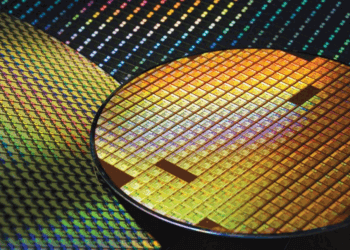
The ecosystem launches with IP partners including Arm, Arteris, eMemory, M31 Technology, Silicon Creations, and Trilinear Technologies, alongside silicon analytics partner proteanTecs. On the manufacturing side, Cadence is working with Samsung Foundry to deliver a silicon prototype demonstration on Samsung’s SF5A process, integrating partner IP to lower adoption risk and provide a reference path from specification through packaged silicon.
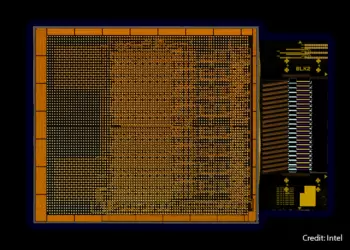
Cadence said the platform combines spec-driven automation, standards-compliant chiplet frameworks, and a full EDA flow spanning simulation, emulation, and physical implementation. The architecture supports Arm Chiplet System Architecture alignment and future OCP Foundational Chiplet System Architecture efforts, while leveraging UCIe for die-to-die connectivity and protocol IP including LPDDR6/5X, DDR5-MRDIMM, PCIe 7.0, and HBM4. Cadence also confirmed that an earlier base system chiplet—integrating its framework, UCIe 32G, and LPDDR5X—has already completed silicon validation.
- Pre-validated chiplet ecosystem covering IP, EDA flows, and packaging
- Initial partners include Arm, Arteris, eMemory, M31 Technology, Silicon Creations, Trilinear Technologies, and proteanTecs
- Silicon prototype collaboration with Samsung Foundry on the SF5A process
- Standards-aligned architectures supporting Arm CSA, UCIe, and emerging OCP frameworks
- Target markets include physical AI, data center, cloud, automotive, and HPC systems
“By combining our extensive IP and SoC design expertise with pre-integrated and pre-validated IP from our robust partner ecosystem, Cadence is accelerating the development of chiplet-based solutions and helping customers mitigate risk,” said David Glasco, vice president of the Compute Solutions Group at Cadence.
🌐 Analysis
The launch reinforces Cadence’s push beyond tools into platform-level enablement as chiplets move from early adoption toward mainstream deployment in AI and data center designs. Similar ecosystem plays from foundries and IP vendors suggest growing alignment around UCIe and standardized chiplet frameworks as the industry looks to manage cost, yield, and scalability at advanced nodes.