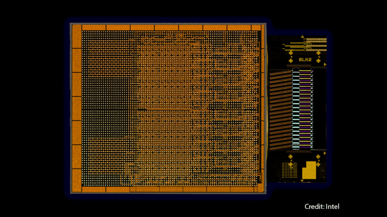
Intel Foundry presented a 300 mm gallium nitride (GaN)-on-silicon chiplet platform at the IEEE International Electron Devices Meeting (IEDM) 2025, highlighting an ultra-thin GaN chiplet with a 19 micrometer silicon base and integrated digital control logic on the same die. IEDM is one of the semiconductor industry’s premier technical conferences, where companies and research teams disclose peer-reviewed breakthroughs in transistor technology, materials, and device physics. Intel’s paper positions GaN chiplets as a path to improve power efficiency, switching speed, and integration density across data center, RF, and wireless infrastructure applications.
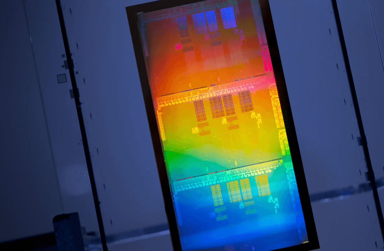
The work centers on combining GaN power transistors with silicon-based logic directly on the same chiplet, eliminating the need for a separate companion control chip. Intel fabricated the devices on 300 mm GaN-on-silicon wafers and thinned the substrate to 19 μm using stealth dicing before grinding. The resulting devices demonstrated voltage blocking up to 78 volts and RF cut-off frequencies exceeding 300 GHz, while also supporting a full set of digital building blocks including inverters, NAND gates, multiplexers, flip-flops, and ring oscillators. Intel reported inverter switching speeds of 33 picoseconds with consistent performance across the wafer.
Intel said the integration approach enables more compact and efficient power delivery systems by reducing interconnect losses between control logic and power devices. The company also highlighted successful reliability testing across TDDB, pBTI, HTRB, and HCI stress conditions, indicating readiness for real-world deployment. Target applications include point-of-load power in AI data centers, 5G and emerging 6G RF front ends, as well as radar, satellite communications, and photonics systems.
- Intel demonstrated a GaN chiplet with a 19 μm silicon base on 300 mm wafers
- Integrated GaN power devices and silicon logic on a single die
- Achieved 78 V blocking voltage and >300 GHz RF cut-off frequency
- Built full digital logic library directly on the GaN chiplet
- Reported 33 ps inverter switching delay across wafer-scale testing
- Positioned for data center power delivery, RF systems, and advanced wireless
“Researchers at Intel Foundry have demonstrated a first-of-its-kind GaN chiplet technology built on 300 mm GaN-on-silicon wafers,” said Han Wui Then, senior principal engineer at Intel Foundry Technology Research, noting the integration of “fully monolithic on-die digital control circuits” using a single manufacturing flow.
🌐 Analysis: IEDM serves as the industry’s proving ground for transistor and materials innovation, often signaling technologies that could enter production over the next 3–7 years. Intel’s GaN chiplet work aligns with its broader foundry strategy that emphasizes heterogeneous integration, advanced packaging, and system-level optimization for AI infrastructure rather than focusing solely on leading-edge logic nodes.
🌐 Analysis: The integration of power and control on the same chiplet reflects a broader shift in AI system design, where power delivery efficiency and proximity to compute become critical constraints. Competing approaches from power semiconductor vendors and hyperscalers also target higher-density voltage regulation and compound semiconductors, but Intel’s use of 300 mm silicon-compatible manufacturing could offer a scaling advantage if it translates to volume production.