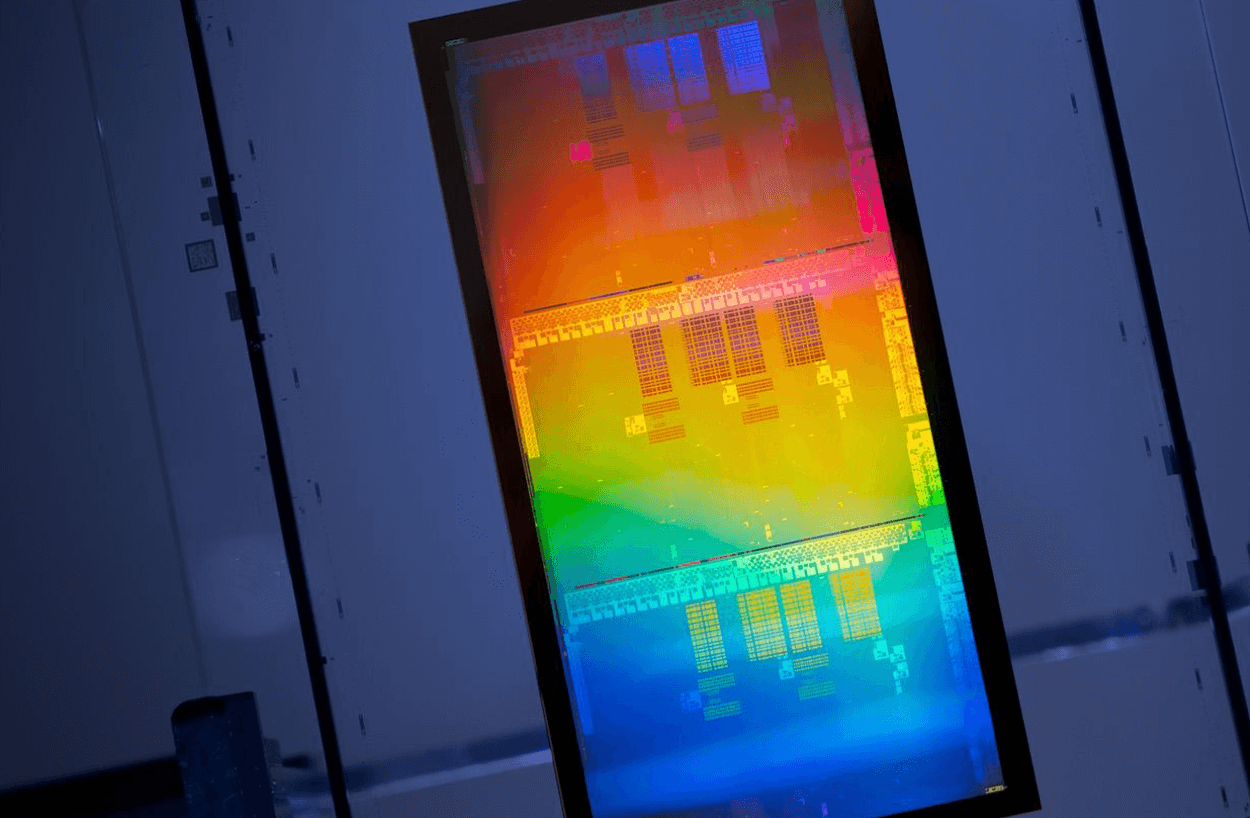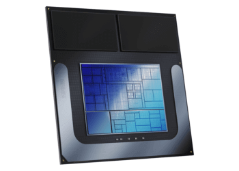

Intel Foundry has begun high-volume manufacturing of a subset of its Intel Core Ultra Series 3 (“Panther Lake”) processors using ASML’s High NA EUV lithography, marking the first commercial shipment of a high-volume logic product manufactured with High NA EUV technology. The production uses ASML’s EXE High NA EUV platform on selected layers of Intel’s 18A process technology, with Intel reporting that those layers are now dual-qualified on both the High NA EUV and conventional NXE EUV platforms. Intel says product is already shipping to customers with yields comparable to production on the NXE platform.
The milestone represents the first production deployment of ASML’s High NA EUV lithography beyond research and pilot manufacturing. Intel and ASML stated that the initial deployment focuses on selected Intel 18A layers, allowing both companies to gather manufacturing data on system uptime, process control, and production implementation while maintaining manufacturing flexibility. Intel said qualifying both NXE and EXE platforms on the same process layers enables increased production output while providing optionality for future process nodes.
Intel installed the industry’s first commercial High NA EUV system at its Hillsboro, Oregon, development facility in 2024 and later became the first customer to accept ASML’s second-generation TWINSCAN EXE:5200B platform. The newer system improves throughput, overlay accuracy, and light source performance compared to the original EXE:5000. ASML positions High NA EUV as the next major advancement in semiconductor lithography, enabling finer patterning required for future AI processors and other advanced semiconductor devices.
• Intel Foundry has entered high-volume manufacturing for selected Panther Lake processors using ASML High NA EUV.
• Production uses selected layers of the Intel 18A process.
• Intel reports yields comparable to production using conventional NXE EUV tools.
• Intel 18A process layers are now dual-qualified on both High NA EXE and NXE platforms.
• Intel says products manufactured using High NA EUV are shipping to customers.
• Deployment utilizes ASML’s EXE High NA EUV platform.
• Intel previously installed the industry’s first commercial EXE:5000 system and later accepted the first EXE:5200B production system.
• The EXE:5200B increases throughput, overlay accuracy, and light source performance.
• Intel and ASML will continue evaluating broader High NA EUV deployment for future process nodes.
“By qualifying the High NA EUV process option on select Intel 18A product layers, our existing fleet of tools are providing customers with increased output, while we develop future options to achieve leading-edge performance, density and manufacturing flexibility on upcoming nodes,” said Naga Chandrasekaran, Executive Vice President and General Manager of Intel Foundry.
🌐 Analysis
This announcement moves High NA EUV from development into commercial semiconductor manufacturing, representing a significant milestone for the advanced lithography roadmap. While Intel is limiting initial deployment to selected process layers rather than the entire chip, the production qualification provides an important validation of High NA EUV manufacturing readiness and offers valuable operational data before broader deployment on future technology nodes.
The announcement also reinforces Intel Foundry’s strategy of serving as the lead manufacturing partner for next-generation lithography technologies. Other leading-edge foundries, including TSMC and Samsung, continue evaluating High NA EUV for future nodes, but Intel is the first to announce shipment of high-volume logic products manufactured using the technology. Broader industry adoption will depend on manufacturing economics, throughput improvements, and customer requirements for future AI and high-performance computing devices.