Qnity Electronics announced the launch of its Advanced Packaging Innovation Hub, a new online platform highlighting the company’s materials and process technologies for advanced semiconductor packaging. The initiative reflects Qnity’s strategy to expand its role in enabling AI, high-performance computing, networking, cloud, and edge computing systems as semiconductor innovation increasingly shifts beyond traditional transistor scaling.
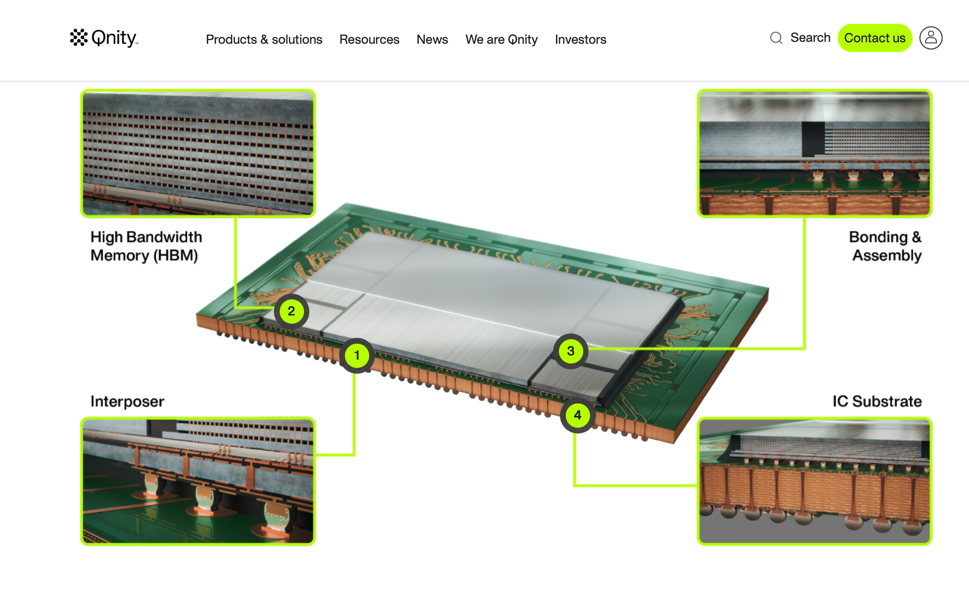
The company positions advanced packaging as a key enabler of next-generation computing architectures, where performance gains increasingly depend on integrating multiple chiplets, memory stacks, and heterogeneous dies into tightly coupled systems. Qnity’s portfolio addresses critical areas across the advanced packaging ecosystem, including High Bandwidth Memory (HBM), interposers, IC substrates, advanced bonding technologies, metallization processes, and assembly solutions.
As AI accelerators and networking processors grow in complexity, manufacturers face challenges involving high-density interconnects, through-silicon vias (TSVs), fine-line redistribution layers (RDLs), hybrid bonding, thermal management, and multi-die integration. Qnity said its materials and process technologies help customers improve manufacturing yields, process control, reliability, and performance while addressing the growing complexity of advanced packaging workflows.
• Launched an Advanced Packaging Innovation Hub highlighting semiconductor materials and process technologies.
• Focused on enabling AI, HPC, cloud, networking, and edge computing platforms.
• Supports key advanced packaging technologies including HBM integration, interposers, IC substrates, TSVs, RDLs, hybrid bonding, and multi-die architectures.
• Targets manufacturing challenges related to yield optimization, defect reduction, thermal management, high-density routing, and long-term reliability.
• Positions advanced packaging as a strategic growth area as the semiconductor industry transitions from transistor scaling (“shrink”) toward heterogeneous integration and 3D stacking (“stack”).
“As AI reshapes computing, the hardest engineering problems are moving into the connections between chips, layer to layer — where performance, power, density, and reliability are decided,” said Chuck Xu, President of Interconnect Solutions at Qnity. “That’s where Qnity shines. We bring our semiconductor and interconnect strengths together so customers can master advanced packaging from design through system integration, end-to-end.”
🌐 Analysis
Advanced packaging has emerged as one of the most strategically important segments of the semiconductor industry as AI workloads drive demand for larger compute clusters and higher memory bandwidth. While leading-edge process nodes continue to advance, many performance gains now come from integrating multiple chiplets, HBM stacks, optical interfaces, and specialized accelerators into a single package. Industry leaders including TSMC, Intel Foundry, Samsung, Amkor, SK hynix, Micron, Broadcom, NVIDIA, AMD, and Marvell have all increased investments in packaging technologies such as CoWoS, EMIB, Foveros, hybrid bonding, and 3D die stacking.
For networking and AI infrastructure, packaging has become a system-level differentiator. The transition to chiplet architectures, co-packaged optics, HBM4 memory, and multi-die AI accelerators is creating demand for advanced materials, substrates, thermal solutions, and interconnect technologies. Qnity’s emphasis on the materials layer reflects a broader industry trend in which performance bottlenecks increasingly reside in the connections between chips rather than within individual silicon dies.
🌐 We’re tracking the latest developments in networking silicon. Follow our ongoing coverage at: https://convergedigest.com/category/semiconductors/
| Profile: Qnity Electronics | |
| Updated | June 2026 |
| Headquarters | Wilmington, Delaware, USA |
| Corporate Origin | Independent public company formed from DuPont’s Electronics & Industrial segment, bringing together semiconductor materials, interconnect technologies, and advanced packaging capabilities under a standalone entity focused on electronics markets. |
| Spinout Milestone | Completed separation from DuPont in 2025, creating a dedicated electronics materials company serving semiconductor manufacturing, advanced packaging, AI infrastructure, and high-speed connectivity markets. |
| Business Focus | Materials, interconnect technologies, and process solutions across the semiconductor value chain. |
| Target Markets | AI infrastructure, HPC, networking, cloud, edge computing, and advanced semiconductors. |
| Core Technology Portfolio | Semiconductor materials, electronic interconnects, circuit materials, advanced packaging process technologies, thermal management, and system integration solutions. |
| Packaging Technologies | HBM integration, TSVs, RDLs, interposers, hybrid bonding, advanced substrates, and multi-die packaging. |
| Key Manufacturing Areas | Metallization, assembly, defect reduction, thermal management, process control, and reliability engineering. |
| Industry Trend Alignment | Transition from monolithic SoCs to chiplets, 2.5D integration, and 3D stacked architectures. |
| AI Infrastructure Relevance | Supports packaging requirements for HBM-equipped AI accelerators, networking ASICs, optical interconnects, co-packaged optics, and heterogeneous computing platforms. |
| Competitive Landscape | Competes across portions of the advanced packaging materials ecosystem alongside companies such as DuPont, Resonac, Ajinomoto, Henkel, Mitsui Chemicals, Shin-Etsu Chemical, and specialty packaging suppliers serving AI semiconductor manufacturing. |
| Latest Announcement | Launch of the Advanced Packaging Innovation Hub showcasing end-to-end solutions for HBM, hybrid bonding, advanced substrates, TSVs, and next-generation AI system integration. |