Synopsys has introduced the first commercial products that combine its electronic design automation (EDA) software with Ansys multiphysics technology, marking a significant milestone less than a year after closing its acquisition of Ansys. The new Multiphysics Fusion portfolio integrates physics-based analysis directly into chip design workflows, enabling engineers to account for power integrity, signal integrity, thermal effects, electromagnetic interactions, and packaging constraints earlier in the design process.
The initial release targets several critical stages of advanced semiconductor development, including timing signoff, design closure, multi-die architectures, and analog and photonic design. Synopsys said the technology combines its AI-powered EDA platforms with Ansys “golden signoff” analysis tools to help reduce costly overdesign while improving design convergence. The company cited customer engagements with Cisco, MediaTek, NVIDIA, and Samsung Foundry as validation of the approach. Reported benefits include up to 3x faster multiphysics timing analysis, up to 10x faster design closure, and concurrent thermal, power, and electromagnetic analysis across multi-die packages.
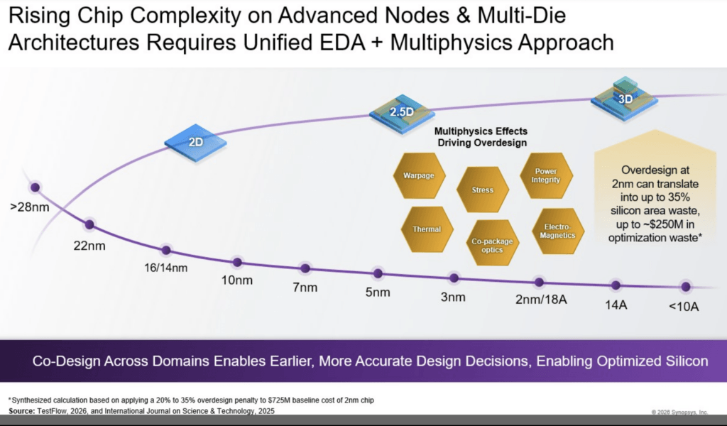
The announcement reflects growing industry demand for system-level co-design as AI accelerators become increasingly dependent on advanced packaging technologies such as 2.5D and 3D integration. Synopsys noted that multiphysics considerations now extend beyond traditional silicon design to include packaging, interconnects, photonics, and co-packaged optics. The new portfolio also incorporates GPU acceleration using NVIDIA CUDA-X libraries, including cuDSS, to accelerate simulation workloads that have become computationally intensive at advanced process nodes.
• Multiphysics Fusion for Timing Signoff combines PrimeTime, RedHawk-SC, RedHawk-SC Electrothermal, StarRC, and HFSS-IC to incorporate IR drop, thermal, and stress effects into timing analysis.
• Multiphysics Fusion for Design Closure integrates PrimeClosure and RedHawk-SC to embed power integrity into signoff optimization, improving ECO success rates and power-performance-area (PPA) outcomes.
• Multiphysics Fusion for Multi-Die Designs combines Synopsys 3DIC Compiler with Ansys multiphysics technologies to provide concurrent analysis of power, thermal, and electromagnetic interactions across advanced packages.
• Multiphysics Fusion for Analog & Photonic Design integrates Custom Compiler with HFSS-IC and combines OptoCompiler with Lumerical to support photonic ICs and co-packaged optics development.
“Multiphysics is fundamentally reshaping how advanced semiconductor designs are engineered, driving a shift from costly overdesign to integrated, system-aware co-design,” said Sanjay Bali, Senior Vice President of EDA Product Management and Strategy at Synopsys.
🌐 Analysis
The release provides one of the clearest examples yet of Synopsys’ integration strategy following its acquisition of Ansys. While EDA vendors have traditionally focused on logical and physical chip design, AI processors increasingly require simultaneous optimization across silicon, packaging, power delivery, thermal management, photonics, and system-level integration. The combination of Synopsys design tools and Ansys simulation technology aims to move multiphysics analysis from a late-stage verification activity into a continuous design methodology.
The inclusion of photonic design and co-packaged optics workflows is particularly notable. Synopsys is positioning the combined Synopsys-Ansys platform not only for traditional semiconductor design but also for emerging AI infrastructure architectures that integrate optical interconnects directly with compute packages. This places the company at the intersection of several major industry trends: AI accelerators, advanced packaging, silicon photonics, and heterogeneous chiplet-based systems.
🌐 We’re tracking the latest developments in networking silicon. Follow our ongoing coverage at: https://convergedigest.com/category/semiconductors/