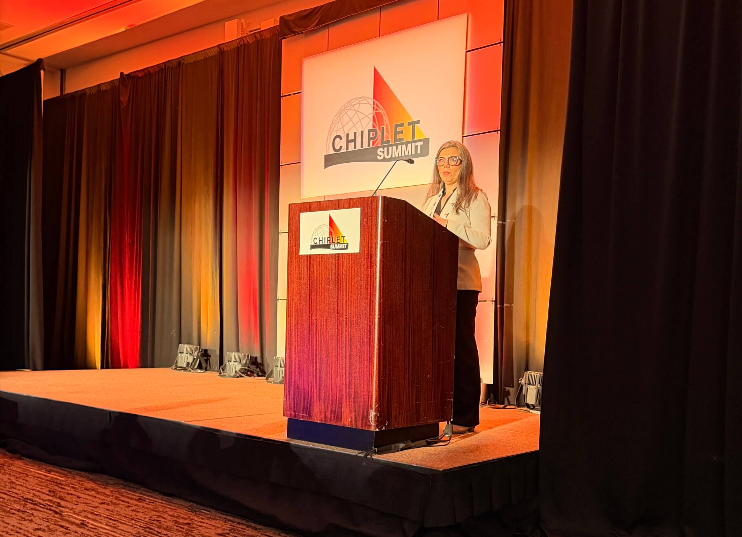
Santa Clara, Calif. — Feb. 18, 2026 – At today’s Chiplet Summit 2026, AlphawaveSemi — now part of Qualcomm — underscored that connectivity has shifted from an enabler to the core architectural requirement for chiplet-based systems. In her keynote, Letizia Giuliano traced chiplet adoption from early proof-of-concept to mainstream deployment and argued that system-level connectivity, power-efficient interconnects, and architectural modularity are now essential for scaling AI infrastructure effectively.
From Promise to Foundation: Chiplets and Connectivity
Giuliano opened by noting that what began as a promising approach has rapidly become the architecture shaping the semiconductor industry. She highlighted steep increases in AI compute demand — with spending projected to more than quadruple in the decade ahead — underscoring the urgency of system-level design thinking. Connectivity is no longer just within a die; it is the defining constraint between dies in a multi-chiplet package, affecting bandwidth, latency, and power budgets in ways that cannot be ignored. Achieving optimal power efficiency, predictable signal integrity, and scalable throughput requires architects to design systems holistically rather than optimizing individual chips in isolation.
She described how, over the last few years, the narrative has shifted: early discussions at the first Chiplet Summit focused on why chiplets matter — now they focus on how to build scalable, reliable, multi-vendor systems. Standardization efforts such as the Universal Chiplet Interconnect Express (UCIe) have evolved (with versions 2.0 and now 3.0), ecosystem participation has grown, and multiple industry players have demonstrated high-volume, interoperable connectivity subsystems.
Connectivity Is Now the Primary System Constraint
Giuliano outlined several system-level challenges that define today’s chiplet era:
- System-level connectivity scaling — Beyond intra-chip interconnects, designers must now manage inter-die data rates, predictable latency, and low power, demanding new methodologies for signaling, integrity, and protocol efficiency.
- Mechanical and test challenges — As packages shrink interconnect distances but increase density, manufacturing issues such as vibration, calibration, and multi-die synchronization rise in complexity.
- Protocol and interface scaling — Modern systems combine compute, memory expansion (e.g., HBM), host interfaces (like CXL), and scale-out connectivity; each protocol places unique demands on link layers and packaging.
- Modular and flexible architectures — The diversity of protocol speeds, link topologies, and packaging types precludes one-size-fits-all solutions; flexible, modular chiplet architectures that can be customized per use case are now essential.
These trends reflect a major shift: designers must now think in terms of systems of chips rather than individual chips, with connectivity as both the primary limiter and the key enabler of performance and power efficiency.
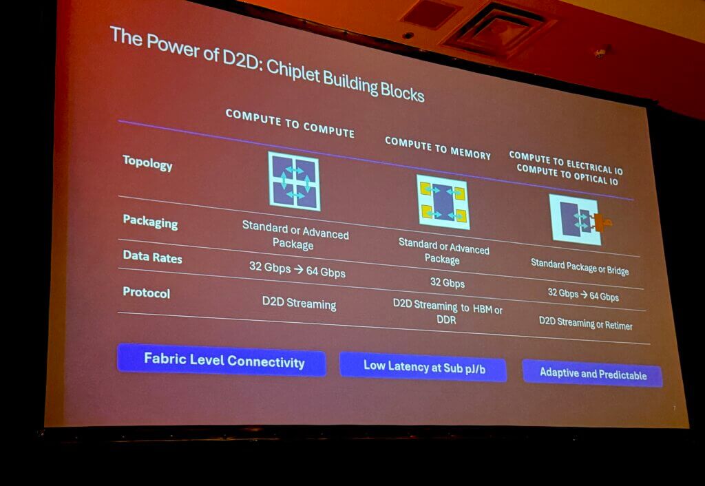
Multi-Generational Die-to-Die Interfaces and Real-World Deployment
Giuliano walked through Alphawave’s evolution of die-to-die connectivity silicon, referencing multiple generations of high-speed interfaces. Early UCIe designs — initially at ~24 Gbps — have progressed through higher bandwidths (e.g., 56 Gbps) and are now deployed at ~64 Gbps per lane, offering power-efficient, predictable channel models across technology nodes and packaging types (including advanced 2.5D/3D integration). These interfaces support a variety of protocols and topologies, enabling compute-to-compute, compute-to-memory, and deeper scale-out connections within and between packages.
She emphasized that system designers must balance power and latency, noting that high-speed data movement consumes significant energy — meaning architectural choices such as partitioning, voltage regulator placement, and protocol selection directly impact both power and performance. Flexible die-to-die fabrics with predictable latency and low energy per bit are essential, particularly as industry data rates scale beyond 64 Gbps and new use cases emerge.
Chiplets Enable the Next Wave: Electrical and Optical Integration
Looking ahead, Giuliano argued that chiplets are the mechanism by which both electrical and optical connectivity will be integrated into next-generation AI systems. Electrical chiplets are evolving alongside optical chiplets — including near-package optics (NPO) — to bring high-bandwidth, low-power links closer to compute elements. By collapsing interconnect distances and reducing electrical overhead, these approaches help mitigate power walls and support ever-larger heterogeneous systems without exceeding physical limits.
She also noted that future architectures will increasingly leverage 3.5D stacking and hybrid integrated fabrics, where chiplets, memory, and optics coexist within the same package to deliver extreme compute density and energy efficiency. This trend underscores her key point: the package is becoming the new motherboard, and connectivity at every level — electrical, protocol, mechanical, and power — must be engineered as part of the system.
In closing, Giuliano urged the industry to embrace the realities of the chiplet era: connectivity is fundamental, system design is paramount, and architectural innovation must account for scalability, reliability, power, and interoperability. The winners in this era will not be those who simply choose the smallest node or largest monolithic die, but those who can integrate diverse components into cohesive, power-efficient, scalable systems within advanced packages.