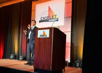
Santa Clara, Calif. — Feb. 18, 2026 — At today’s Chiplet Summit 2026, Debendra Das Sharma, **Chair of the UCIe Consortium, laid out how Universal Chiplet Interconnect Express (UCIe) is evolving into the industry’s foundational standard for on-package connectivity, enabling heterogeneous chiplet systems to scale bandwidth, power efficiency, and interoperability for AI and high-performance computing.
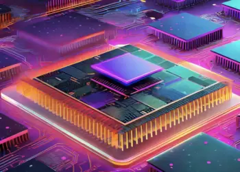
Das Sharma framed chiplets as a response to multiple converging pressures: reticle limits, rising costs and yield challenges for large monolithic dies, exploding IP porting costs, and the growing need to place high-bandwidth memory closer to compute. Together, these forces are pushing the industry toward smaller, reusable dies assembled into advanced packages—turning the package itself into the new locus of system innovation.
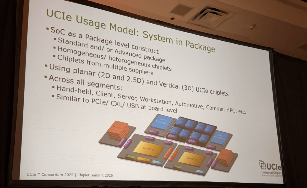
Package as the New Platform
A central theme of the keynote was that the package is becoming the new platform—and the new SoC. Just as PCIe and CXL created open innovation slots at the board level, Das Sharma argued that chiplets require an open, interoperable standard inside the package to avoid vendor lock-in and to enable mix-and-match integration of compute, accelerators, memory, I/O, analog, and emerging optical functions.
UCIe was designed around principles learned from decades of standards work:
- Openness and a level playing field
- Backward-compatible evolution to protect long-term investments
- Optimized power-performance across the full compute continuum, from mobile to AI/HPC
- Continuous evolution to meet future architectural demands
Today, the UCIe Consortium counts 140+ member companies, spanning semiconductor vendors, IP providers, foundries, packaging houses, and cloud service providers, organized through working groups covering electrical, protocol, form factor, compliance, software, manageability, security, and automotive use cases.
From Planar to 3D: The UCIe Roadmap
Das Sharma walked through three major generations of UCIe development, emphasizing that each step has been member-driven and backward compatible, while expanding scope beyond raw interconnect into operability at the package and system level.
| UCIe Generation | Scope & Key Capabilities |
|---|---|
| UCIe 1.0 | Fully specified, layered die-to-die interconnect for planar (2D / 2.5D) packaging. Defines PHY, sideband, clocking, channel, die-to-die adapter, and protocol mappings (PCIe, CXL, streaming) to ensure multi-vendor interoperability. |
| UCIe 1.1 | Backward-compatible enhancements adding new usage models, automotive-oriented health monitoring, and cost-optimization options for advanced packaging. |
| UCIe 2.x | Introduces UCIe-3D for vertical chiplets using hybrid bonding, plus package-level infrastructure for testability, manageability, debug, and field serviceability. |
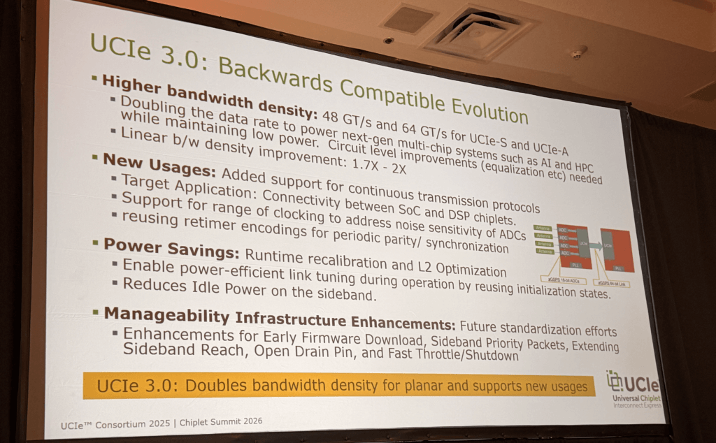
| UCIe 3.0 | Doubles data rate to 64 GT/s to address AI/HPC and on-package memory bandwidth, adds continuous transmission protocol mappings, and expands sideband and manageability capabilities while maintaining backward compatibility. |
A major technical inflection highlighted in the keynote was UCIe-3D, which standardizes vertical chiplet integration using hybrid bonding. With near-zero inter-die distance and aggressively shrinking pitch, 3D chiplets unlock orders-of-magnitude increases in bandwidth density compared to planar approaches.
Rather than pushing links to ever higher frequencies, Das Sharma emphasized a “wider, not faster” philosophy: more wires, shorter distances, lower frequencies, and dramatically lower power per bit. In this regime, die-to-die communication can approach the energy efficiency and latency of on-die interconnect, effectively making a 3D stack behave like an extension of a monolithic chip.
Analysis: Why UCIe Matters for AI and On-Package Memory
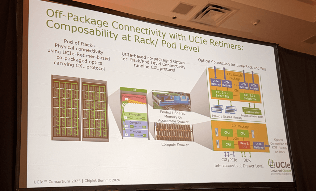
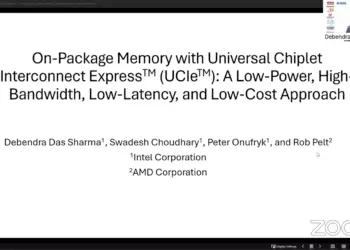
Throughout the talk, Das Sharma repeatedly tied UCIe’s evolution to AI-driven memory bandwidth pressure. As accelerators scale, feeding compute becomes the dominant constraint—and board-level I/O cannot deliver the required bandwidth density or energy efficiency. UCIe’s move to 64 GT/s, combined with dense planar links and ultra-dense 3D integration, is aimed squarely at preventing on-package memory and chiplet fabrics from becoming the bottleneck.
Equally important, the keynote stressed that raw bandwidth alone is insufficient. AI systems demand operability at scale: robust test, debug, manageability, and secure update paths for chiplets that may be inaccessible once packaged. By extending UCIe beyond the interconnect into package-level infrastructure, the consortium is addressing real deployment needs—from manufacturing test through field service—without fragmenting the ecosystem.
Das Sharma concluded that UCIe is a multi-decade standard, still early in its journey but already demonstrating interoperability across vendors and process nodes. The industry’s challenge now is not whether chiplets will succeed, but how effectively standards like UCIe can enable scalable, power-efficient systems as AI continues to push against the limits of physics.