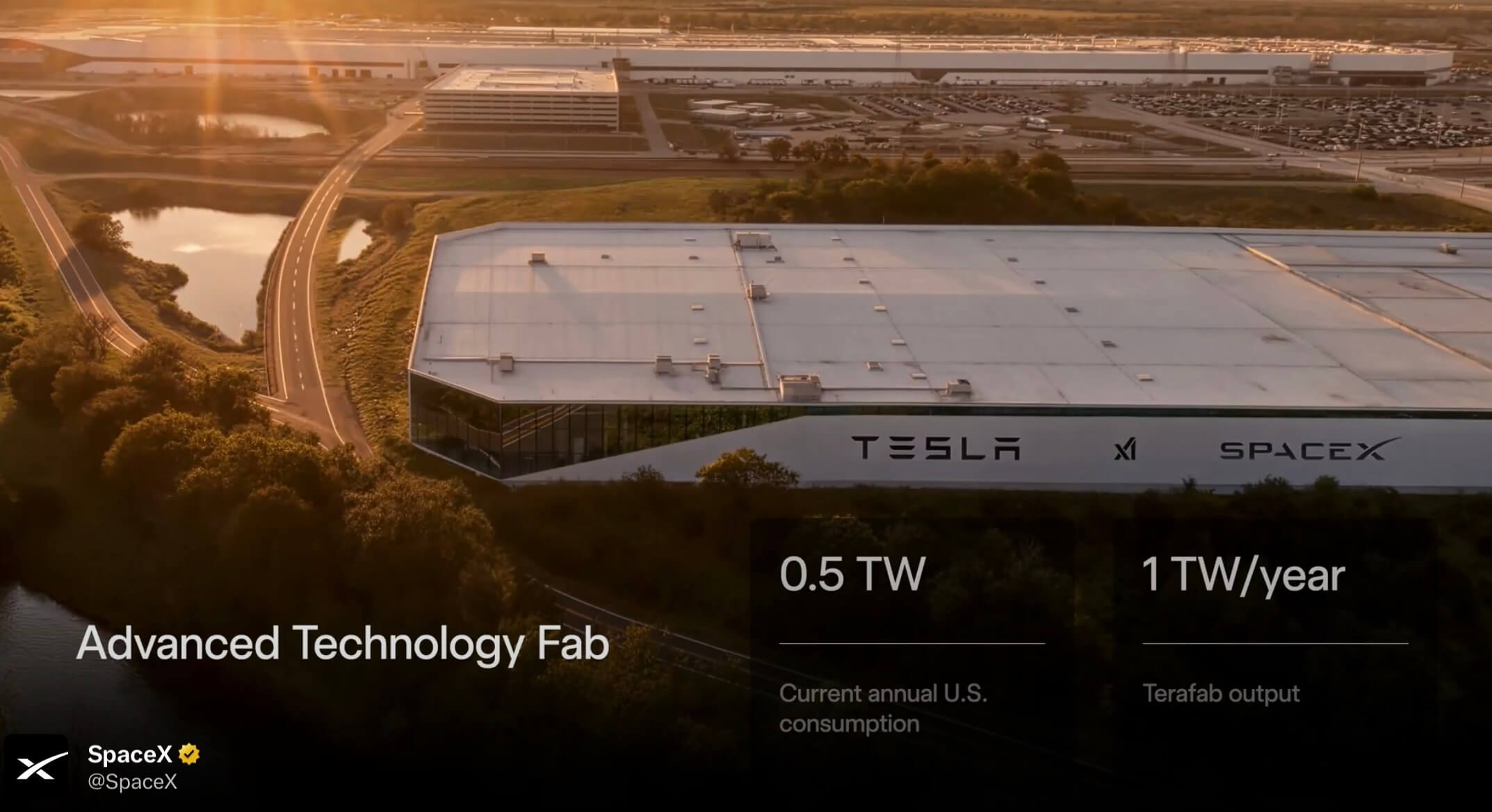
Tesla has detailed an aggressive expansion of its Terafab initiative, outlining plans for a vertically integrated semiconductor facility in Austin designed to address what it sees as a fundamental shortfall in global AI chip production. Speaking at the inaugural Terafab launch event, CEO Elon Musk positioned the fab as essential infrastructure to support Tesla’s long-term AI, robotics, and compute ambitions. The company is moving forward with an advanced technology fab in Texas that will consolidate chip design, manufacturing, testing, and packaging into a single, tightly integrated environment.
Musk described Terafab as a response to a widening gap between global semiconductor output and projected demand for AI compute. He estimated that current worldwide chip production capacity represents only a small fraction—on the order of a few percent—of what would be required to support Tesla’s long-term compute goals. Tesla will continue sourcing chips from partners including TSMC, Samsung, and memory suppliers, but indicated that external supply alone cannot scale fast enough. “We will buy all the chips our suppliers can produce,” Musk noted, “but it’s still not enough—so we have to build Terafab.”
The Austin facility will serve as the foundation of this strategy, with a design that integrates lithography mask creation, wafer fabrication, packaging, and validation into a single building. This architecture enables rapid, iterative development cycles—allowing Tesla to design, fabricate, test, and refine chips in a continuous loop. Musk emphasized that this closed-loop model could significantly accelerate innovation compared to conventional semiconductor workflows that rely on geographically distributed steps. The fab is expected to produce both inference-optimized chips for edge applications such as vehicles and humanoid robots, as well as higher-performance processors designed for more demanding compute environments.
- Terafab will be located in Austin, Texas, near Tesla’s Gigafactory Texas
- Fully integrated fab: lithography masks, wafer fabrication, packaging, and testing in one facility
- Designed for rapid iteration with tight design-to-production feedback loops
- Targets both edge inference chips (vehicles, Optimus robots) and high-performance AI processors
- Addresses projected global shortfall in AI chip supply capacity
- Complements, rather than replaces, existing suppliers such as TSMC and Samsung
- Early hiring underway for fab construction, infrastructure, and manufacturing roles
“It’d be crazy not to try out the Terafab,” said Elon Musk, CEO of Tesla.