
Advanced Chip and Circuit Materials (ACCM) introduced Celeritas SMC, a silicon-matched core material for advanced IC substrates designed to reduce warpage and thermomechanical stress in large AI, HPC, chiplet, and embedded-bridge packages. ACCM said the material matches the in-plane coefficient of thermal expansion (CTE) of silicon while using established organic-substrate manufacturing processes. The company manufactures Celeritas SMC at its facility in Wisconsin and is shipping material for customer evaluations.
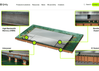
The new core targets a growing materials challenge as advanced package dimensions increase beyond 100 mm per side and designers embed silicon bridge dies within substrates. Conventional organic cores typically have an in-plane CTE of 12 to 16 ppm/°C, compared with roughly 3 ppm/°C for silicon. ACCM said Celeritas SMC provides tunable silicon-matched CTE from room temperature to 100 °C, a glass transition temperature above 300 °C, 0.004 dissipation factor at 10 GHz, 0.1% moisture absorption at saturation, and core thicknesses ranging from 100 to 1,200 µm and above.
ACCM positions Celeritas SMC as an alternative to glass-core substrates that does not require through-glass vias (TGVs), glass-specific metallization, specialized panel handling, or new substrate fabrication equipment. Fabricators can form vias using standard mechanical and laser drilling, laminate industry-standard build-up films directly to the core, and process panels using installed substrate manufacturing lines. ACCM also offers tunable-CTE PCB materials ranging from 2 to 10 ppm/°C, supporting graded CTE architectures from silicon dies and package substrates through system boards.
• Target applications: large-body AI accelerator packages, HPC processors, chiplet architectures, embedded silicon bridges, and other advanced IC substrates.
• Silicon-matched CTE: Tunable construction designed to match silicon between room temperature and 100 °C.
• Thermal performance: Glass transition temperature above 300 °C for package assembly and rework thermal budgets.
• Electrical performance: Dissipation factor of 0.004 at 10 GHz, with lower-loss grades available.
• Moisture absorption: 0.1% at saturation.
• Thickness range: 100 to 1,200 µm and above.
• Manufacturing compatibility: Supports mechanical drilling, laser drilling, standard lamination, conventional panel handling, and established substrate fabrication equipment.
• Domestic manufacturing: ACCM produces Celeritas SMC at its Wisconsin facility.
• Commercial availability: Material is shipping and available for immediate customer evaluation.
“The industry does not have a low CTE problem, it has a low CTE at acceptable cost problem,” said Tarun Amla, PhD, Founder, President, and CEO of ACCM. “Glass core asks the entire substrate supply chain to retool around through-glass vias before volume yields and economics have been established. Celeritas SMC gives packaging engineers silicon-matched CTE, high stiffness, and low loss on the equipment they already own, with the drilling, metallization, and lamination processes they already know. That is the difference between a roadmap concept and a material customers can put on their lines today.”
🌐 Analysis: Celeritas SMC enters the advanced packaging materials market as AI accelerator and HPC package dimensions increase and substrate warpage, dimensional stability, and interconnect reliability become more difficult to manage. ACCM’s strategy differs from glass-core development programs by targeting silicon-like CTE while retaining compatibility with existing organic-substrate manufacturing infrastructure, but broad market adoption will depend on customer qualification, volume manufacturing yields, long-term reliability data, and integration with advanced packaging supply chains.